By Ian Darney
There have been many designs of common-mode rejection circuits in the pages of EW over the past sixty years, but this is the first which takes into account the characteristics of the interconnecting wires. Another unique feature is the use of transient, rather than frequency, analysis. Transient analysis covers the entire range, from DC to GHz.
A systematic approach is applied to the design process, similar to the use of library models in SPICE software to simulate the behaviour selected integrated circuits on printed circuit board assemblies.
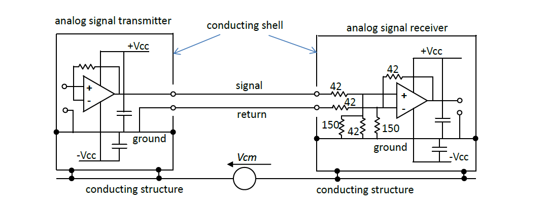
Given the availability of a circuit model of the signal link, it becomes possible to tailor the design of the interface circuitry of the signal receiver to maximise common-mode rejection. The design is basically the same as that adopted for a twin-conductor transmission line; terminate the link with resistors equal to the characteristic resistances of the conductors.
The simulation shows how the receiver performs in the presence of a high level of transient interference.
General Circuit Model
The starting point to the design process is the General Circuit Model of the configuration under review. For transient analysis, this is as illustrated by Figure 1. It consists of three sections;
the interface circuitry of the signal source at the near end of the link,
the signal link, comprising the send, return, and ground conductors,
the interface circuitry of the signal receiver at the far end.
The resistors Ro1, Ro2 and Ro3 simulate the characteristic resistance of each conductor. The resistors Rs1, Rs2 and Rs3 represent the series resistances of the circuitry at the signal source interface.
All the currents are defined as loop currents; forward along the upper conductor and back along the lower conductor: that is, clockwise. Ini1, Inr1 and Ina1 are the incident, reflected and absorbed currents in the differential-mode loop at the near end. Ini2, Inr2 and Ina2 are the incident, reflected and absorbed currents in the common-mode loop. Initially, the incident currents at the near end are set at zero.
When a step voltage is applied to the differential-mode terminals, current Inr1 flows forward along Rs1 and Ro1, then back along Ro2 and Rs2. This creates a voltage in the common-mode loop, thus inducing a current Inr2.
The cable is represented as a series of sections. Currents Inr1 and Inr2 manifest themselves as discrete charges which propagate from section to section along the cable; and this can be simulated using two shift registers. The differential-mode loop is represented by n1 sections, the common-mode loop by n2 sections. This caters for the fact that the velocities of propagation in the differential-mode loop and common-mode loops are different.