By James Stanbridge, Regional Manager, JTAG Technologies UK
For many the term “JTAG” is still a point of confusion; for some engineers it is a device-programming port while for others it is for plugging in a microprocessor emulator or debugger, whereas, in fact, it was originally devised for neither. JTAG is an acronym of “Joint Test Action Group”, and initially the aim was to provide an alternative system to aid circuit board assembly testing, i.e. for detecting and diagnosing assembly errors such as solder shorts, lifted pins and missing/badly-placed components. The Group in JTAG refers to a small number of test professionals who met over a period of four to five years from 1985, to devise a scheme to embed test circuitry into digital devices with the aim of assisting in the structural test of PCBA(s). Similar schemes had been developed unilaterally by device manufacturers, such as IBM’s LSSD, but at that point there was no interoperability standard that all vendors could comply to. By 1990, the JTAG system, also known as “boundary-scan”, was officially an IEEE standard number 1149.1.
Alternative Uses
Soon after its formal introduction, however, alternative uses for JTAG appeared, such as a (firmware) debugger port and a device programming port. This hi-jacking of the JTAG port can be attributed to silicon companies like Texas Instruments and ARM, who both considered the compact four-wire interface and state-machine could be used to access internal (debug) registers, as well as the IEEE standard 1149.1 test registers defined by the JTAG committee. At this point it might have been useful to define a new name for this class of activity, so that along with the original “JTAG for board test” use there was also “JTAG for embedded debug” – although, in fact, the latter is not covered by the IEEE standard.
To confuse matters even further, in 1993 Intel introduced a range of PLDs that were one of the first to use the JTAG port for directly accessing configuration/programming registers for the logic fabric. As a result, now there’s also “JTAG for programming”.
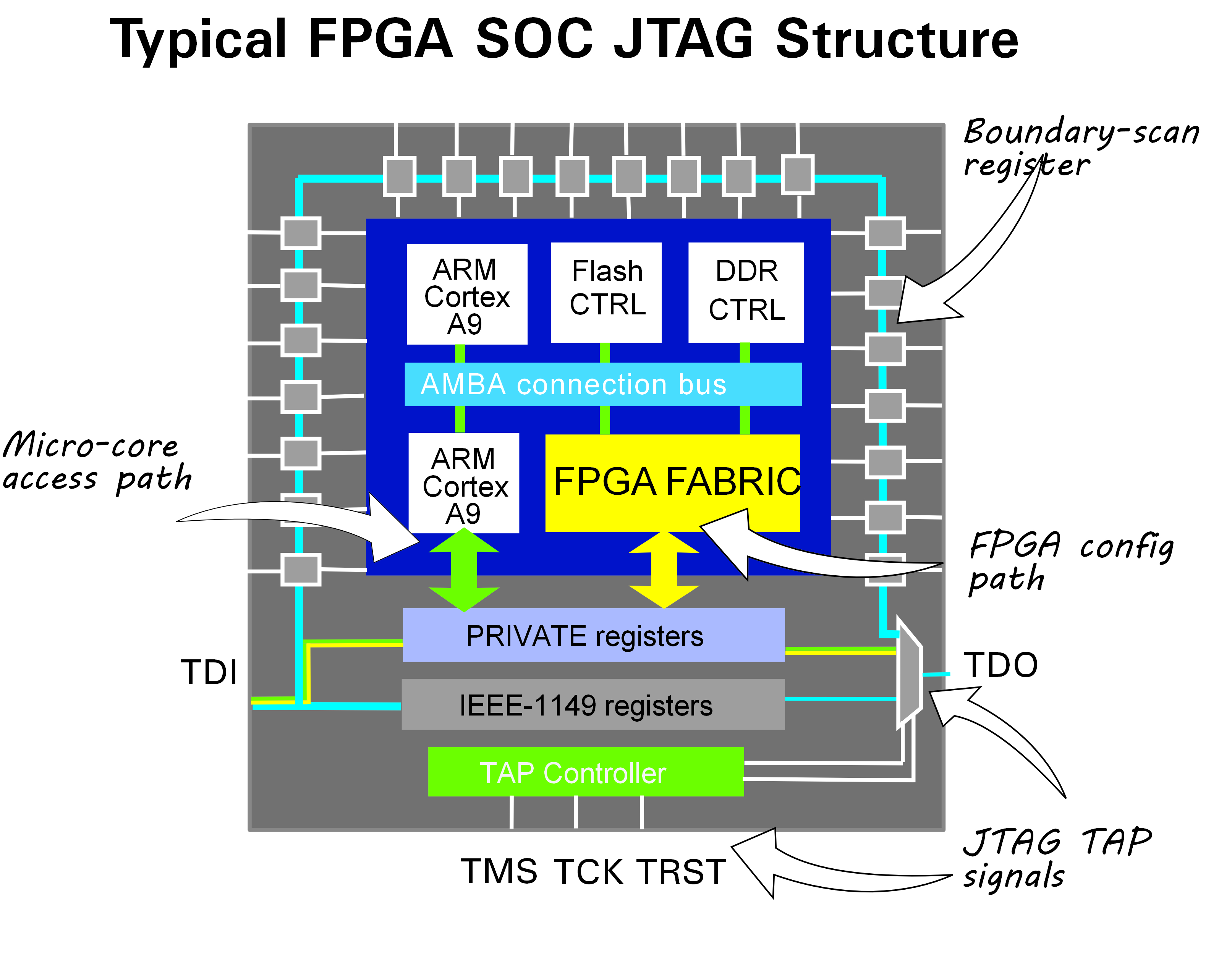
And there it is! Within three years of its formal existence, the JTAG committee’s test port spawned two other applications: RISC/DSP processor debug and device OBP (on-board programming). Twenty years on, and the market now includes devices that feature all three aspects of JTAG. Xilinx Zynq SOCs, for example, contain a processor section with dual ARM A9 cores, plus a programmable section configured by JTAG and a regular IEEE Std 1149.1 boundary-scan sub-system; see Figure 1.

Figure 1: JTAG aspects of a modern FPGA/SOC such as Xilinx Zynq
Evolving Toolsets
At the birth of the standard in 1990, JTAG tools were rather basic and limited to the test aspect. Some ATPG (Automatic Test Program Generators) existed for creating pin-to-pin interconnect tests but still required a significant input of design knowledge from users in order to set safe test conditions on the target design. Memories and logic device (cluster) tests had to wait until the mid-90s, when companies like JTAG Technologies introduced tools including MTPG (Memory Test Program Generator) as add-ons to their existing boundary-scan test programs. Next came the support for in-system programming of CPLDs (Altera, Cypress, Lattice, Xilinx, etc.) and, later still, flash memories. It was at this stage that PCB assembly manufacturers could use a common platform for structural testing and programming of boards prior to the final functional testing stage.
By the end of the 1990s, JTAG/boundary-scan testing and programming was a well-established technique, used widely for early-process fault detection on complex, high-value designs, so much so that some users abandoned conventional structural testers In-Circuit Testers (ICTs)and Manufacturing Defect Analysers (MDAs) in favour of JTAG/boundary-scan. Others, meanwhile, looked for solutions that allowed them to augment their current testers with JTAG – often through third-party bolt-on kits such as JTAG Symphony.
Throughout the 2000s, JTAG/boundary-scan tools were further refined, ease of use reached new levels through extensive device modelling, and support for new JTAG methods such as IEEE 1149.6 (boundary-scan testing of high-speed LVDS connection) was added. However, all that time, there were still few indications that the “JTAG for embedded debug” and embedded test in general would become a more mainstream requirement in the factory.
Using All Facets
By the start of this decade, however, the desire to test boards using all JTAG facets (debug as well as test and programming) was recognised, as test engineers discovered that using capabilities such as embedded processor core-emulation would allow faster and potentially more thorough testing of peripherals like complex DDR-type memories. Furthermore, core access provides the ability to communicate with SOC embedded peripherals like ADCs and DACs. And, so, the highly-desirable aspect of “JTAG-powered analogue testing” can, at last, be realised.
Products such as CoreCommander by JTAGLive offer these capabilities at low cost and even allow FPGAs to be configured with test-specific IP, triggered using the same test equipment as conventional boundary-scan. So-called “Dual JTAG” systems offer a host of testing possibilities due to synchronisation of these assets, especially when controlled by a powerful open-source scripting language such as Python.
The Future
Technology rarely stands still, and since testing has to keep pace with the products being built, JTAG has also been updated. The most recent major updates to standard 1149.1 came in 2013, with a sizable addendum to the original work following a period of intense activity around 2010, with two separate groups proposing similar updates to the existing 1149.1 standard, which was by then 20 years old.
Thus, in addition to 1149.1 2013, another group was working on an on-chip access infrastructure for embedded instruments, aka IEEE 1687. Both groups identified deficiencies in the existing standard and proposed to address these through the introduction of more “dynamic” IC infrastructures. In the case of 1149.1 2013, the driver for the changes was to standardise some of the design practices that IC vendors had introduced on a unilateral basis, such as initialisation protocols, individual device ID codes and power management scenarios. While in the case of 1687 the main driver was to improve board-level ‘testability’ through greater use of embedded test cores (BIST IP) accessed via an extended standardised infrastructure.
The now-ratified extension to 1149.1 includes the syntax of a new procedural description language (PDL) which defines the use of dynamic register segmentation and device IP hierarchy for a given application. IEEE 1687, meanwhile, also features PDL; however, there’s only a basic level of compatibility between the two PDLs – apparently, due to the large differences in focus of each new standard!
PDL is designed to document procedures for stimulating and observing test data register fields for 1149.1-2013 and, in 1687, the procedures for stimulating and observing data to an instrument. Not much of a difference except that in 1687 a second language is required to describe the (embedded instrument) access networks – ICL (Instrument Control Language), whereas in 1149.1-2013 the access network descriptions are embedded in an extended BSDL model. For complex networks that make extensive use of embedded instruments 1687s ICL is claimed to be better suited.
A Very Versatile Port
The JTAG committee’s boundary-scan test access port started out in life over 25 years ago as a facility for production/test engineers to aid in fault-finding on surface mounted PCBAs. Since then, applications for this versatile port have grown and the value to both design and test engineers increased. Whilst designers can enjoy cheap and easy access to their microprocessor’s debug registers, test and production engineers can get a low-cost versatile on-board device programmer coupled to their structural tester right at the point of assembly.
Be aware, however, that not all standards make the cut; we’ve already seen the analogue variant (1149.4) wither on the vine. Only time will tell if the newcomers 1149.1-2013 and 1687 will gain sufficient traction and buy-in from the semiconductor houses, to make them as ubiquitous as the original format.

Figure 2 – Summary/examples of JTAG-powered board test option on a modern digital or mixed-signal design.
- Scan Path Infrastructure
- Boundary-scan device ó device interconnections including external test module (DIOS)
- Boundary-scan cluster testing and programming [of non JTAG devices]
- JTAG (IEEE Std.1149.6) AC-EXTEST testing of ac-coupled LVDS signals via loop-back
- Testing using JTAG CoreCommander – controls device embedded peripherals to test DRR at-speed, plus ADC inputs and Ethernet PHY.
- Embedded memory programming using JTAG CoreCommander