By Robert Hillinger, Business Development Manager, Kistler Group
The advance of 5G, IoT and Big Data, as well as new technology introductions, place greater demands on semiconductors. As application requirements become more complex, so does the need for better performing-semiconductors, in turn making their production more challenging.
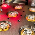
Conventional approaches to process control, such as using optical and displacement sensors in combination with electrical testing, can’t keep up with these demands. However, measurement of dynamic force with piezoelectric sensors has proven to be an effective method to control production processes. The applied process force is a critical factor in manufacturing semiconductors, both in front-end processes such as wafer grinding, polishing, CMP or delamination, and in back-end processes including lead frame stamping, die, wire and wafer bonding, sealing and sorting. Deviations in the applied force during these processes mean mechanical stress, which can lead to quality issues. Force measurement is therefore an important parameter for achieving tighter process control and avoiding mechanical stress, caused, for instance, by tool wear, changing material behavior or machine malfunctions in semiconductor production; it enables users to correlate force signals to certain product quality parameters.
Piezoelectrical force measurement
Force measurement with piezoelectric sensors has shown to be a highly-efficient method for monitoring, controlling and optimising semiconductor production. The operation principle is based on the piezoelectric effect, where piezoelectric (PE) materials such as quartz crystals generate linearly-proportional electrical charge in response to pressure. High linearity means highly-accurate measurements, in the range of 0.1N to 100kN.
Another advantage is that the PE effect occurs in the direction of the force, and diagonally as a shear effect, allowing PE sensors to be integrated in various ways in an application. Due to their rigidity, they are highly responsive to rapid force changes.
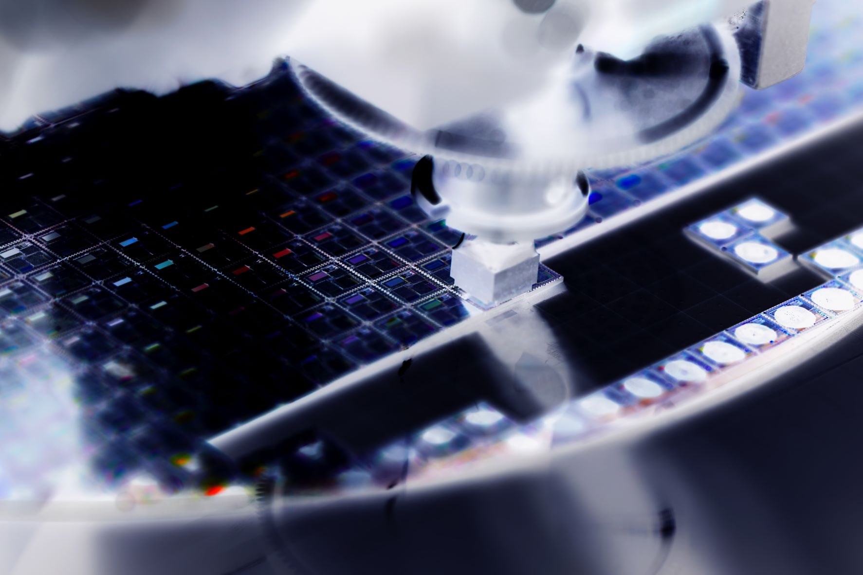
PE sensors are not used as single measuring units, but as a part of a measurement setup. For example, a PE sensor measures the force, a charge amplifier converts it and provides the programmable logic controller (PLC) or industrial PC with a signal equal to that measured force; see Figure 1.

Figure 1: PE load washer sensor with charge amplifier and programmable logic controller
Software allows each production step is visualised by a curve (either force/time or displacement), making it easy to check for quality. Users can additionally adapt the curve evaluation to the individual monitoring task by using evaluation objects. With this approach, every production step can be checked to determine whether the part is bad or good.
Besides process monitoring hardware and software, Kistler offers a broad range of PE sensors and charge amplifiers. Users can select the most suitable sensors according to the application and available space. The best-fitting charge amplifier can be chosen depending on the number of channels, measurement range and type (static/dynamic), analogue or digital output signal, and frequency range. Besides a carefully-chosen design and components of the measurement chain, good measurement practices include avoiding acceleration and temperature changes during measurement. If they can’t be avoided, it is necessary to implement measures to overcome their influence. Furthermore, users should provide good cable insulation and routing, as well as compensate the reset/operate jump, for instance with the maXYmos evaluation system from Kistler or a PLC.
Inline measurement – i.e., when force sensors are mounted in the mechanical structure of the semiconductor equipment – offers important possibilities. Together with the charge amplifier and process evaluation unit, inline sensors enable users to record and assess the applied force. They can optimise the production process based on the collected assembly data. As inline measurement chains allow for measuring and recording the force of every production step, they are suitable for the automatic inspection of mass-produced items, which also entails traceability for each produced item.
Accurate measurements
Resolution is defined as the ability of the measurement system to detect and accurately indicate small changes in the characteristic of the measurement result. Even with forces as low as 1N, PE force measurement can achieve resolutions of less than 0.01N. In addition, PE measurement comes up with quality levers such as repeatability or serial precision, which allows for determining the accuracy of repeated measurements between identical production steps. Users can take advantage of this and use relative instead of absolute measurement.
In the past, piezoelectric force measurement technology was mainly used for machine verification and highly-accurate wire bonding, wafer grinding and polishing. Today, the technology is used in a growing number of applications throughout the semiconductor industry – in front-end and back-end processes, as well as in testing processes such as sorting and taping; see Table 1.
Manufacturers profit from these sensors’ long lifespan and compact sizes. The benefits for production itself are manifold: it improves machine performance regarding speed and accuracy, increases the quality of the produced items, thus reducing the ppm failure rate and, ultimately, decreases costs.
| Manufacturing process step | Force measurement integration | |||
| Features | Benefits | Added values | ||
| Front end | PolishingGrindingCMPDicingLaminationDelaminationHandling | Improve down force precision and control, e.g. with wafer polishing headsMonitor forces applied during lamination and pick-and-placeTrace force during critical production processes | Verify flatness and force limitationsIdentify wear on machine parts such as pressure platesEnsure consistent performance during wafer polishing, grinding, cleaning, dicingReduce wafer defects | Increased machine performance, e.g., speed and accuracyIncreased quality and reduced costs |
| Back end | Lead frame stampingDie bonderWire bonderFlip chipWafer bondingThermo-compression bondingSinteringDie sortingSealingMolding | Improve bonding precision by full-loop bonder head control with force measurementMonitor forces applied during bonding and/or pick-and-place processes, and othersCavity pressure monitoringTrace force in critical semiconductor processes | Keep the critical physical variable of force within allowed tolerances during bonding and pick-and-placeVerify flatness, parallelismIdentify wear on machine partsReduce die defects | |
| Testing | Bond pull strength testerSorting and tapingTest handler (pick-and- place, turret) | Check bond forceMonitor force during pick-and- place processes | Identify deviationsEnsure process safety |
Table 1: Semiconductor manufacturing processes where force measurements are required