The most remarkable aspect of technology is its constant development and improvements. Today, laptops and smartphones are slimmer and smaller, and medical devices are designed to be unobtrusive and barely visible to the naked eye.
As electronic devices continue to evolve and shrink, so do their circuits and, ultimately, their components. This trend has led to the demand for component miniaturisation. 3D circuits, also known as “3D-MID”, or three-dimensional mechatronic integrated devices, make this possible. They enable more compact designs whilst enhancing their functional density.
The miniaturisation revolution in electronics
Smaller devices also means lower environmental impact. A laptop, for example, uses 80% less power than a desktop computer, with peak power consumption of 60W compared to 175W for desktops. This reduction in energy use is due to miniaturisation.
Miniaturisation has revolutionised many sectors, from medical and healthcare to automotive, not to mention consumer and industrial electronics. Here are a few drivers for the trend:
- Aesthetics:
Users expect devices to be visually appealing and well-designed.
- Portability:
Users also want devices to be lightweight and easy to carry.
- Low power consumption and eco friendliness:
Users are increasingly looking for devices with low power consumption in their effort reduce their impact on the environment. Smaller parts consume less energy which helps lower operating costs, increase battery life and promote greener products.
- Less heat dissipation
Since smaller parts use less power, electronic devices generate less heat. This means bulky heatsinks or fans can be removed, reducing power, weight, noise and cost.
* Cost savings
Whilst miniaturisation can be initially costly, it uses fewer materials, which saves money in the long run.
3D-MID
Almost every industry is moving toward functional density, meaning that hardware components must be smaller and interconnected. 3D-MID can fulfil these requirements by reducing volume and optimising space whilst adding more functionalities to parts.
The term “mechatronics” was coined in 1969 by a senior engineer of the Japanese firm Yaskawa. It is a combination of the words “Mecha” (machines) and “Tronics” (electronics).
Since then, the definition has evolved. It is now used to describe the abilities to use computers, electronics and mechanics to build integrated and more intelligent systems, such as robotic, control and electromechanical systems.
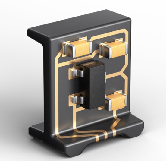
3D-MID stands for “Three-Dimensional Moulded Interconnect Device” or “Three-Dimensional Mechatronic Integrated Device”, combining electronic and mechanical functionalities into a single three-dimensional component.
Harting’s 3D circuits technology allows 3D-MID parts or injection-moulded thermoplastic parts to be integrated with electronic circuits and components, making them more compact and functionally dense. Imagine a circuit board that is significantly smaller and composed of plastic rather than metal.
Furthermore, injection-moulded circuit boards significantly reduce the number of production processes and individual components, reducing assembly time and hence lowering production costs.
Designing with 3D-MID
The flexibility of 3D-MID technology allows device designers to go where they need to. A three-dimensional component that combines electrical and mechanical functions allows for endless possibilities.
The designers lay down their requirements along with very specific measurements. The components are then constructed through injection moulding, which is the process of heating materials such as plastic and melting them before being injected into a mould and cooled to achieve the desired shape. It is a process often used by many industries because it can create complex shapes parts quickly for mass production.
Because injection moulding is so flexible, designers can use it to construct virtually anything with exact specifications. Before realising a mould, different forms of simulation can be used to check if the parts fulfill the requirements and that sample parts can be made for rapid prototyping.
Next comes laser activation through laser direct structuring (LDS), a procedure created by LPKF Laser & Electronics in 1996. It is where a laser beam defines the conductive trace, etching the layout directly into the injection-moulded plastic component.
The injection-moulded plastic will have special additives that laser beams can detect. The lasers then reveal areas where the conductor structures will eventually be placed.
In the chemical plating process, copper only lays down on the laser structured areas, enabling the development of very precise electronic circuits.
After metallisation in a copper bath, conductive traces form in the areas that have been activated and will allow for metals to adhere to it.
3D-MID applications
3D-MID technology is often regarded as a gamechanger in several applications, including sensor devices and miniaturised electronic packaging, LED carriers and lighting modules, and antennas and connectivity modules. In effect, almost all industries can benefit from 3D circuits, since all of them need some form of miniaturisation.
In the medical and healthcare markets, for example, mechatronics is a promising discipline, used in diagnostics and treatment.
For example, in endoscopy – typically a very uncomfortable procedure. With 3D-MID, endoscopy modules are far less invasive and more tolerated by patients. Instead of long endoscopic cameras and tubes, a non-invasive capsule contains a miniature camera that can be easily swallowed, which then transmit 360-degree pictures from inside the body to the doctor.
Mechatronics are also widely used in creating new types of prosthetics, such as the Luke Arm, a mind-controlled arm prosthesis that gives patients who’ve lost limbs the ability to perform everyday tasks.
3D-MID technologies are also used in designing smaller hearing aids, implants and surgical and dental devices.
3D-MID-enabled possibilities go on: As the technology advances, we expect to see more organisations incorporate these circuits in space-saving projects, making devices a lot smaller, with reduced assembly procedures and costs, yet with greater functionality.
By Harting development engineers