By Anthony Desimone, Applications Engineer, and Michael Giancioppo, Applications Engineer, Analog Devices
JESD204B is a recently approved JEDEC standard for serial data interfacing between converters and digital processing devices. As a third-generation standard, it addresses some of the limitations of the earlier versions. Among the benefits of this interface are reductions in required board area for data interface routing, reductions in setup and hold timing requirements, and the enablement of smaller packages for converter and logic devices. New analog/digital converters from various vendors, such as the AD9250 from Analog Devices, use this interface.
There is a trade-off to realizing the benefits of the JESD204B interface, as it has complexities and subtleties that distinguish it from existing interface formats and protocols. As with any standard, it is clear that the interface must function seamlessly to gain popularity and traction vs. more common interfaces, such as single data rate or double data rate CMOS or LVDS. Although the JESD204B standard is documented by JEDEC, some specific information about it is subject to interpretation or may be spread over multiple references. It is also obvious that it would be extremely helpful if there were a concise guide that provided an overview of the standard, how it works, and how to troubleshoot it if issues arise.
This article explains the interface from an ADC to an FPGA for JESD204B, how to identify when it’s working correctly, and, perhaps more importantly, how to troubleshoot it if something isn’t quite right. The troubleshooting techniques discussed can use commonly available test and measurement equipment including oscilloscopes and logic analyzers, along with software tools such as the ChipScope from Xilinx® or SignalTap from Altera®. Interface signaling is also explained to allow a single approach or multiple approaches to visualize the signaling.
JESD204B Overview
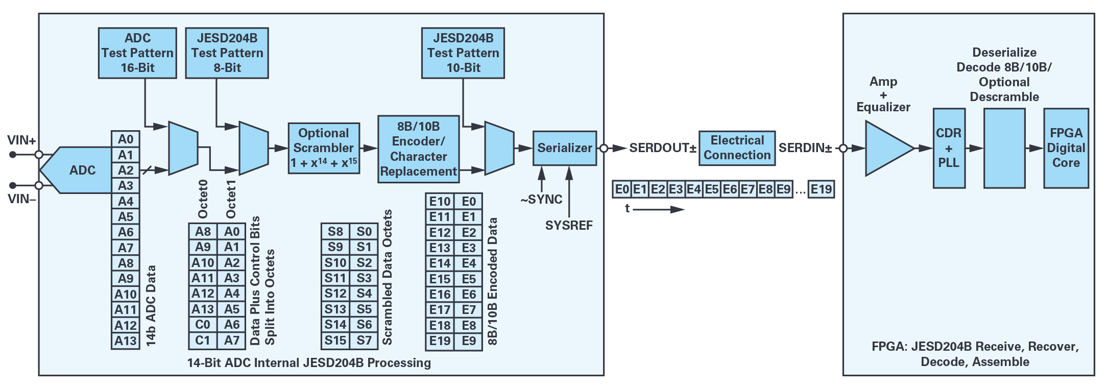
The JESD204B standard provides a method to interface one or multiple data converters to a digital signal processing device (typically, an ADC or DAC to an FPGA) over a higher speed serial interface compared to the more typical parallel data transfers. The interface, which runs at up to 12.5 Gbps/lane, uses a framed serial data link with embedded clock and alignment characters. The interface eases implementation of the data interface of high speed converters by reducing the number of traces between devices, thus reducing trace-matching requirements, and removing setup- and hold-timing constraint issues. Since a link needs to be established prior to data transfer, there are new challenges and techniques required to identify that the interface is working properly and, if not, what to do.
The JESD204B interface uses three phases to establish the synchronized link: code group synchronization (CGS), initial lane synchronization (ILAS), and data transmission phase. The required signals for the link are a shared reference clock (device clock), at least one differential CML physical data electrical connection (called a lane), and at least one other synchronization signal (SYNC~ and possibly SYSREF). The signals used depend upon the subclass:
- Subclass 0 uses device clock, lanes, and SYNC~
- Subclass 1 uses device clock, lanes, SYNC~, and SYSREF
- Subclass 2 uses device clock, lanes, and SYNC~
Subclass 0 is adequate in many cases and will be the focus of this article. Subclass 1 and Subclass 2 provide a method to establish deterministic latency. This is important in applications wherein synchronizing multiple devices or system synchronization or fixed latency is required (such as when a system needs a known sampling edge for an event or an event must react to an input signal within a specified time).
Figure 1 shows a simplified JESD204B link from the transmit device (ADC) to the receive device (FPGA), with data from one ADC going over one lane.
Although there are many variables within the JESD204B specification, some have particular importance when establishing a link. These key variables from the specification are (note that these values are typically represented as “X − 1”):
- M: number of converters.
- L: number of physical lanes.
- F: number of octets per frame.
- K: number of frames per multiframe.
- N and N’: converter resolution and number of bits used per sample (multiple of 4), respectively. N’ value is N value, plus control and dummy bits.
Subclass 0: Synchronization Steps
As noted above, many applications can use the relatively simpler Subclass 0 mode of operation. This is also the easiest mode to establish and for which to verify a link. Subclass 0 uses three phases to establish and monitor synchronization: CGS phase, ILAS phase, and data phase. The figures associated with each phase present the data in different formats, as they might be seen on an oscilloscope, logic analyzer, or FPGA virtual I/O analyzer such as Xilinx ChipScope or Altera SignalTap.
The Code Group Synchronization (CGS) Phase
The most significant parts of the CGS phase that can be observed over the link are shown in Figure 2, along with a description of the five highlighted points of the figure.
- The receiver issues a synchronization request by driving the SYNC~ pin low.
- The transceiver transmits /K28.5/ symbols (10 bits/symbol), unscrambled beginning on the next symbol.
- The receiver synchronizes when it receives at least four consecutive/K28.5/symbols without error and then the receiver drives the SYNC~ pin high.
- Receiver must receive at least four 8B/10B characters without error otherwise synchronization fails and the link stays in CGS phase.
- CGS phase ends and ILAS phase begins.
The /K28.5/ character, also just known as /K/, within the JESD204B standard can be exhibited as shown in Figure 3. The standard requires a running neutral disparity. The 8B/10B coding allows a balanced sequence that, on average, contains an equal amount of 1s and 0s. Each 8B/10B character can have a positive (more 1s) or negative (more 0s) disparity, and the parity of the current character is determined by the current sum of the previous characters sent. This is typically accomplished by alternately transmitting a positive parity word, followed by a negative parity word; the figure shows both polarities of the /K28.5/ symbol.

Figure 1. JESD204B link diagram for one ADC to an FPGA through one lane.

Figure 2. Logic output of JESD204B subclass 0 link signals during CGS phase (assumes two lanes, one device with two ADCs).

Figure 3. Logic output of /K28.5/ characters and how it propagates through the JESD204B Tx signal path.
Note these key points:
- Serial value represents the logic levels of the 10 bits transmitted over the lane, as would be seen by an oscilloscope measuring the physical interface.
- 8B/10B value represents the logic values (10 bits) transmitted over the lane, as might be seen by a logic analyzer measuring the physical interface.
- Data value and data logic represent the logic levels of the symbol inside the JESD204B transceiver block before 8B/10B coding, as would be seen on an FPGA logic analysis tool such as Xilinx ChipScope or Altera SignalTap.
- Symbol represents the hex value of the character that is to be transmitted, noting parity for PHY layer.
- Character is shown to indicate the JESD204B character as it is referred to in the JEDEC specification.
The ILAS Phase
In the ILAS phase, there are four multiframes that allow the receiver to align lanes from all links and also allows the receiver to verify the link parameters. Alignment is required to accommodate trace length differences and any character skew the receivers introduce. Each successive multiframe immediately follows the previous one of four (Figure 4). Whether or not the scrambling link parameter is enabled, ILAS is always transmitted without scrambling.
The ILAS phase begins after SYNC~ has been deasserted (goes high). After the transmit block has internally tracked (within the ADC) a full multiframe, it will begin to transmit four multiframes. Dummy samples are inserted between the required characters so that full multiframes are transmitted (Figure 4). The four multiframes consist of the following:
- Multiframe 1: begins with an /R/ character [K28.0] and ends with an /A/ character [K28.3].
- Multiframe 2: begins with an /R/ character followed by a /Q/ [K28.4] character, followed by link configuration parameters over 14 configuration octets (Table 1), and ends with an /A/ character.
- Multiframe 3: the same as Multiframe 1.
- Multiframe 4: the same as Multiframe 1.
The frame length can be calculated for the JESD204B parameters:
(S) × (1/Sample Rate).
Translation:
(Number of Samples/Converter/Frame) × (1/Sample Rate)
Example:
A converter running at 250 MSPS that has one sample per converter per frame (Note “S” is 0 in this case since it is encoded as binary value –1) has a 4 ns frame length.

(1)
The multiframe length can be calculated for the JESD204B parameters:

(2)
Translation:
(Number of Samples/Converter/Frame) × (Number of Frames/ Multiframe) × (1/Sample Rate)
Example:
A converter running at 250 MSPS that has one sample per converter per frame and 32 frames per multiframes has a 128 ns multiframe length.

(3)
Data Phase with Character Replacement Enabled
In the data transmission phase, frame alignment is monitored with control characters. Character replacement is used at the end of frames. There is no additional overhead to accommodate data or frame alignment during the data phase. Character replacement allows an alignment character to be issued at a frame boundary if and only if the last character of the current frame may be replaced with the last character of the last frame, facilitating (occasional) confirmation that the alignment has not changed since the ILAS sequence.
Character replacement in the transmitter occurs in the following instances:
- If scrambling is disabled and the last octet of the frame or multiframe equals the octet value of the previous frame.
- If scrambling is enabled and the last octet of the multiframe is equal to 0x7C, or the last octet of a frame is equal to 0xFC.
Transmitters and receivers each maintain a local multiframe counter (LMFC) that perpetually counts to (F × K) − 1 and then wraps back to “0” to count again (ignoring internal word width). A common (sourced) SYSREF is issued to all transmitters and receivers that use the SYSREF to reset their LMFCs, after which all LMFCs should be synchronized (within one clock) to each other.
At the release of SYNC (seen by all devices) the transmitter begins ILAS at the next (Tx) LMFC wrap to “0.” If F × K has been properly set to be greater than the (transmit encode time) + (line propagation time) + (receiver decode time), received data will propagate out of the receiver’s SERDES before the next LMFC. The receiver will pass the data into a FIFO, which will begin outputting data at the next (Rx) LMFC boundary. This known relationship between the transmitter’s SERDES input and the receiver’s FIFO output are known as the deterministic latency.

Figure 4. Logic output of JESD204B subclass 0 link signals during ILAS phase.

Figure 5. Figure of /K/ character [K28.5], /R/ character [K28.0], /A/ character [K28.3], and /Q/ character [K28.4].
Table 1. Table of CONFIG (Fourteen JESD204B Configuration Parameters Octets) in ILAS Multiframe 2
| Octet No. | Bit 7 (MSB) | Bit 6 | Bit 5 | Bit 4 | Bit 3 | Bit 2 | Bit 1 | Bit 0 (LSB) |
| 0 | DID[7:0] | |||||||
| 1 | ADJCNT[3:0] | BID[3:0] | ||||||
| 2 | ADJDIR | PHADJ | LID[4:0] | |||||
| 3 | SCR | L[4:0] | ||||||
| 4 | F[7:0] | |||||||
| 5 | K[4:0] | |||||||
| 6 | M[7:0] | |||||||
| 7 | CS[1:0] | N[4:0] | ||||||
| 8 | SUBCLASS[2:0] | N[4:0] | ||||||
| 9 | JESDV[2:0] | S[4:0] | ||||||
| 10 | HD | CF[4:0] | ||||||
| 11 | RESERVED 1 | |||||||
| 12 | RESERVED 2 | |||||||
| 13 | FCHK[7:0] |
What Can Go Wrong?
JESD204B can be a complicated interface standard, with many operational subtleties. Finding out why it is not working requires a good understanding of likely scenarios:
Stuck in CGS mode: if SYNC stays at logic low level; or pulse high for <4 multiframes:
Checking the board, unpowered:
- SYSREF and SYNC~ signaling should be dc coupled.
- With the board unpowered, check that the board SYNC~ connections from the SYNC~ source (typically from the FPGA or DAC) to the SYNC~ input (typically ADC or FPGA) are good and low impedance.
- Check that the pull-down or pull-up resistors are not dominating the signaling, for example, if values are too small or shorted and, therefore, cannot be driven correctly.
- Verify that the differential-pairs traces (and cables, if used) of JESD204B link are matched.
- Verify differential impedance of the traces is 100 Ω.
Checking the board, powered:
- If there is a buffer/translator in the SYNC path, make sure it is functioning properly.
- Check that SYNC~ source and board circuitry (both SYNC+ and SYNC−, if differential) are properly configured to produce logic levels compliant for the SYNC~ receive device. If logic level is not compliant, then review circuitry for source and receive configurations to find the problem. Otherwise, consult device manufacturer.
- Check that the JESD204B serial transmitter and board circuitry are properly configured to produce the correct logic levels for the JESD204B serial data receiver. If logic level is not compliant, review circuitry of source and receive configurations to find the problem. Otherwise, consult device manufacturer.
Checking SYNC~ signaling:
- If SYNC~ is static and logic low, the link is not progressing beyond the CGS phase. There is either an issue with the data being sent, or the JESD204B receiver is not decoding the samples properly. Verify /K/ characters are being sent, verify receive configuration settings, verify SYNC~ source, review board circuitry, and consider overdriving SYNC~ signal and attempt to force link into ILAS mode to isolate link receiver vs. transceiver issues. Otherwise, consult device manufacturer.
- If SYNC~ is static and logic high, verify the SYNC~ logic level is configured correctly in the source device. Check pull-up and pull-down resistors.
- If SYNC~ pulses high and returns to logic-low state for less than six multiframe periods, the JESD204B link is progressing beyond the CGS phase but not beyond ILAS phase. This would suggest the /K/ characters are okay and the basic function of the CDR are working. Proceed to the ILAS troubleshooting section.
- If SYNC~ pulses high for a duration of more than six multiframe periods, the link is progressing beyond the ILAS phase and is malfunctioning in the data phase; see the data phase section for troubleshooting tips.
Checking serial data
- Verify the transceiver’s data rate and the receiver’s expected rate are the same.
- Measure lanes with high impedance probe (differential probe, if possible); if characters appear incorrect, make sure lane differential traces are matched, the return path on the PCB is not interrupted, and devices are properly soldered on the PCA. Unlike the (seemingly) random characters of ILAS and data phase, CGS characters are easily recognizable on a scope (if a high enough speed scope is available).
- Verify /K/ characters with high impedance probe.
- If /K/ characters are correct, the transceiver side of the link is working properly.
- If /K/ characters are not correct, the transceiver device or the board Lanes signal have an issue.
- If dc coupled, verify that the transmitter and receiver common-mode voltage is within specification for the devices
- Depending upon implementation, the transmitter common-mode voltage can range from 490 mV to 1135 mV.
- Depending upon implementation, the receiver common-mode voltage can range from 490 mV to 1300 mV.
- Verify the transmitter CML differential voltage on the data lanes (note that the CML differential voltage is calculated as two times the voltage swing of each leg of the signal).
- The transmitter CML differential voltage can range from 0.5 V p-p to 1.0 V p-p for speeds up to 3.125 Gbps.
- The transmitter CML differential voltage can range from 0.4 V p-p to 0.75 V p-p for speeds up to 6.374 Gbps.
- The transmitter CML differential voltage can range from 0.360 V p-p to 0.770 V p-p for speeds up to 12.5 Gbps.
- Verify the receiver CML differential voltage on the data lanes (note that the CML differential voltage is calculated as two times the voltage swing of each leg of the signal).
- The receiver CML differential voltage can range from 0.175 V p-p to 1.0 V p-p for speeds up to 3.125 Gbps.
- The receiver CML differential voltage can range from 0.125 V p-p to 0.75 V p-p for speeds up to 6.374 Gbps.
- The receiver CML differential voltage can range from 0.110 V p-p to 1.05 V p-p for speeds up to 12.5 Gbps.
- If preemphasis is an option, enable and observe data signals along the data path.
- Verify that the M and L values match between the transmitter and receiver, otherwise the data rates may not match. For example, M = 2 and L = 2 will expect half the data rate over the serial interface as compared to the M = 2 and L = 1 case.
- Ensure the device clock going to the transmitter and receiver is phase locked and at the correct frequency.
Can not get beyond ILAS mode if SYNC pulses high for approximately four multiframes:
- Link parameter conflicts
- Verify link parameters are not offset by 1 (many parameters are specified as value −1).
- Verify ILAS multiframes are transmitting properly, verify link parameters on the transceiver device, the receiver device, and those transmitted in ILAS second multiframe.
- Calculate expected ILAS length (tframe, tmultiframe, 4 × tmultiframe), verify ILAS is attempted for approximately four multiframes.
- Verify all lanes are functioning properly. Ensure there are no multilane/ multilink conflicts.
Get into data phase but occasionally link resets (returns to CGS and ILAS before returning to data phase):
- Invalid setup and hold time of periodic or gapped periodic SYSREF or SYNC~ signal.
- Link parameter conflicts.
- Character replacement conflicts.
- Scrambling problem, if enabled.
- Lane data corruption, noise, or jitter could force the eye diagram to close.
- Spurious clocking or excessive jitter on device clock.
Other general tips when troubleshooting link:
- Run converter and link at the slowest allowed speed, as this allows use of lower bandwidth measurement instruments that are more readily available.
- Set minimum allowed combinations of M, L, K, S.
- Use test modes when possible.
- Use Subclass 0 for troubleshooting.
- Disable scrambling while troubleshooting.
This troubleshooting guide cannot be all inclusive but provides a good basic baseline for an engineer working with and wanting to learn about a JESD204B link.
This summary of the JESD204B specification provides practical information about the link. Hopefully, engineers getting involved with this latest high performance interface standard will find it informative and helpful if troubleshooting is required.