By Graham Mostyn, Applications Engineering Manager, Microchip Technology
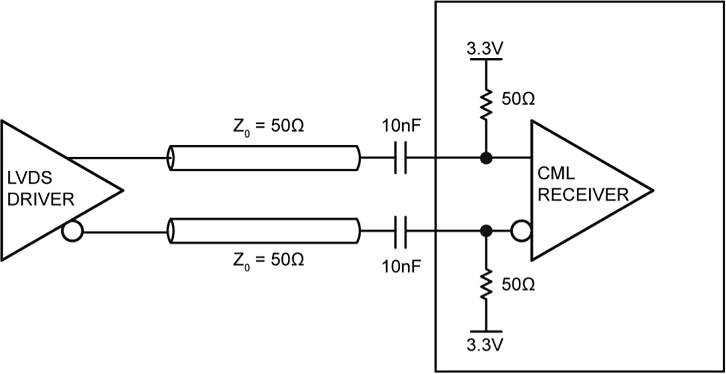
Each type of clock logic features a different common-mode voltage and swing level; see Table 1. Because of these differences, clock logic translation needs to be implemented between the driver and receiver sides in system design. This article describes how to translate one type of differential clock logic into another by adding attenuation resistors and bias circuits between them to attenuate the swing level and re-bias the common-mode for the input of the receiver.
However, prior to designing a logic translation circuit, a solid understanding of the input/output structures of each type of clock logic is necessary.
LVPECL Input/Output Structure
Logic low-voltage, positive-referenced, emitter-coupled logic (LVPECL) originates from emitter-coupled logic (ECL), adopting a positive power supply. The LVPECL input is a current-switching differential pair with high input impedance; see Figure 1. The input common-mode voltage should be approximately Vcc − 1.3V to allow operating headroom, either from internal self-biasing or external biasing.