The TTL crystal oscillator circuit is one of the simplest circuits electronic circuit designers can build; see Figure 1. However, despite its simplicity and stable performance, it has a fundamental problem – it can’t generate a pure sinusoidal signal, but a slightly distorted one, regardless of the frequency; see Figure 2.

Figure 1: A typical TTL crystal oscillator circuit
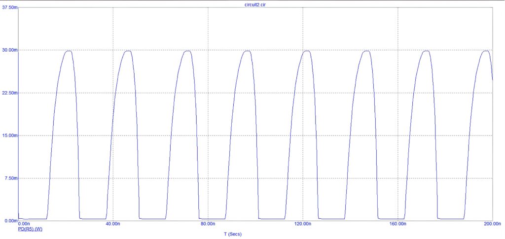
Figure 2: TTL circuit output signal
Signal distortion can be measured by the Total Harmonics Distortion (THD) indicator. So, the question is, what are the best operating criteria that keep THD at its lowest level for the TTL crystal oscillator circuit? We will find out with the following experiment.
The experiment setup
For the experiment we used different values for the load resistor R5 (Figure 1), logging the output voltage signal generated by the circuit and its THD.
We assumed the following:
- Throughout this experiment, R1, R2, R3, R4 and the crystal were kept unchanged, to allow proper monitoring of the impact of load resistance changes on the output voltage THD.
- The power supply was also kept constant, to avoid interfering with the collected data.
Figure 3 shows the THD values versus the load resistance values. As it can be seen, the THD is kept low when R5 is between 3Ω and 86Ω; beyond this range (9.2kΩ -9.5kΩ), the THD is much higher.
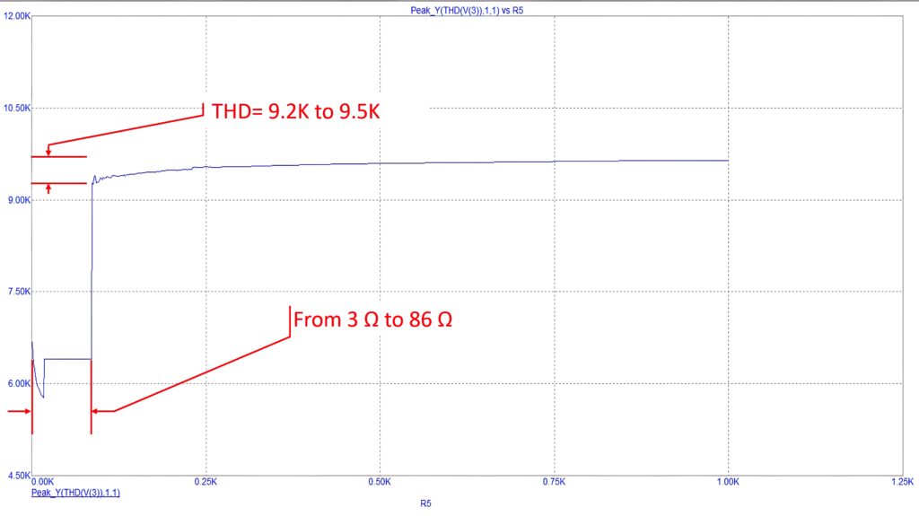
Figure 3: THD against various load resistances
In addition, Figure 3 shows that the lowest possible THD value of the output signal can be obtained when R5 is 17Ω.
We can conclude that the load resistance (R5) is better in terms of generated harmonics when it is between 3Ω and 86Ω, and at its best when it is 17Ω.
But, this is not the end of the story. In theory, the load resistance of any electronic circuit is sized to be equal to the circuit’s output resistance to ensure the load receives the maximum power from the circuit. This is fundamental for all circuits delivering power to their connected load, which begs another question: What is the optimum load resistance value within the permitted low THD range?
More to it
To answer this question, the power delivered across the load resistance, R5, was measured at various load resistance values. This power can be multiplied by the RMS value of the voltage and current across resistor R5; see Figure 4, which shows the output power varying with the R5 value. It can be concluded that the maximum load delivered across the load resistor, R5, is about 25.7Ω.
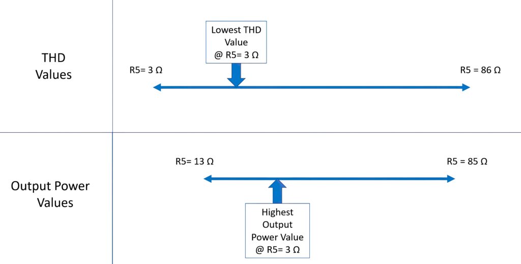
Figure 4: Output power vs. load resistance
Figure 5 summarises all the findings from this experiment. Unfortunately, the value of the load resistance that grants the optimum power delivery differs from that of the load resistance for the lowest THD. This is an important finding, since we should not blindly design oscillator circuits to maximise the power delivery to the load only, but should also consider the THD performance. Consequently, as an electronic circuit designer, you need to pay attention to both factors in your design, and select the one most important for the application. Is a less distorted output signal more important than the maximum output power, or vice versa? This experiment sheds light on the demanding decision electronic circuits designers must make before assembling their circuits.