New materials with exciting properties are constantly being proposed for microelectronics applications, but there is a challenge: a lack of understanding about how they perform under real-world environmental conditions.
As the demand for microelectronics continues to increase, electronic design and development engineers face numerous challenges, such as reducing energy consumption, increasing battery storage capacity whilst shortening battery charging times, and incorporating sustainable materials – at the same time reducing the size and weight of components. Solutions to many of these challenges can be found by considering advanced novel materials, such as energy-efficient semiconductors, organic photovoltaics, 2D coatings for sensitive components, and ultra-thin semiconductors and insulators.
Unlocking the benefits of these materials requires a deep understanding of their properties, particularly how their performance or stability varies under the environmental conditions found in real-world applications. Such sample characterisation can be done using well-established techniques such as Raman, FT-IR and X-ray spectroscopy, using instrument stages that allow experiments to be carried out under a range of conditions of temperature, atmosphere and vacuum pressure.
Here we will discuss two applications where being able to precisely control the temperature of the material using this approach has made a significant contribution to understanding its properties.
Studying crystallographic phase transitions
X-ray diffraction (XRD) generates diffraction patterns that are correlated directly with the presence of certain components in a material, giving a picture of the phases present and defect details.
XRD was historically used to examine crystalline materials, but two refinements of the technique are now frequently used to study non-crystalline or semi-crystalline materials in powdered or liquid form. Wide-angle X ray scattering (WAXS) measures scattering at 2θ angles of > 5°, and provides structural information down to 0.1nm, similar to traditional XRD.
Small-angle X ray scattering (SAXS) measures scattering at 2θ angles of 0-5°, and provides information on complex molecules and materials such as polymers, colloids and porous materials, with a feature size of up to 500nm.
The Centre for Nature-Inspired Engineering (CNIE) at the Department of Chemical Engineering of University College London has a SAXS/WAXS system. It is fitted with several stages to vary the conditions under observation, including a regular temperature-controlled stage for experiments to be conducted between –175°C and 350°C, and a capillary X-ray stage for observing small volumes of materials at temperatures from 4°C to 80°C.
The set-up at CNIE has been used to detect new polymorphs and phase changes in both solid and liquid samples. A good example of this is the analysis of two phase transitions in pyroglutamic acid (PGA); see Figure 1. It was found that the low-temperature phase change, from the α′ to the α phase, happens slowly and appears to be martensitic (a hard and very brittle solid solution) in character, in which the strain at the α–α′ interface in partially transformed crystals caused the transformation to occur in bursts. Applied to the microelectronics field, this opens up the prospect of detecting new polymorphs and phase changes in novel materials that might have consequences for real-world applications.
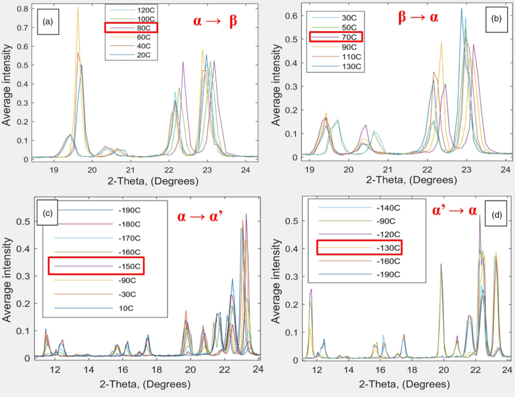
Figure 1: WAXS data for PGA acquired using a temperature-controlled capillary stage, showing the forward and reverse phase changes at (a, b) 80°C and 70°C (fast transition) and (c, d) -150°C and -130°C (slow transition). Data was collected over a period of 2s at temperature intervals of 10°C
The protective effect of 2D coatings for copper
The components of electronic circuits must be protected as much as possible from environmental stresses, and materials that are one atomic layer thick – 2D materials – are now receiving attention for this purpose because they do not affect the morphology of the substrate.
Graphene is one such material, which has the desirable property of being highly impermeable to liquids, gases and chemicals. However, it has high electronic conductivity, which could create a galvanic cell if placed in contact with a conductor, potentially causing degradation over time. Therefore, hexagonal boron nitride (hBN), which has the same permeability as graphene and does not form a galvanic cell, has been studied as an alternative.
A study carried out at the Micro and Nanotechnology Department at the Technical University of Denmark, Copenhagen, compared the protective properties of graphene and hBN under two oxidation environments using Raman spectroscopy. This uses a laser beam to study the vibrational modes of molecules, and so provides a ‘fingerprint’ enabling compound identity to be uncovered.
The study generated layers of the materials on copper through chemical vapour deposition, and examined their properties under two oxidation environments, one short-term and one long-term. The results from the short-term study (Figure 2) indicated graphene to be an effective barrier. However, between 150°C and 300°C, hBN was less effective, which was believed to be due to the higher density of grain boundaries and wrinkles, which are known to induce faster oxidation of the copper substrate.
Another observation was that above 300°C, the oxidation of the graphene coating increased, as measured by the increase in the Raman intensity of the CuO and Cu2O peaks, which were seen to be larger than for hBN.
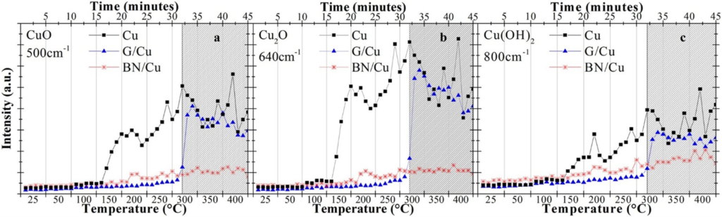
Figure 2: Short-term oxidation study: Evolution of the Raman signal intensity for (a) CuO at 500 cm−1, (b) Cu2O at 640 cm–1, and (c) Cu(OH)2 at 800 cm−1 on bare copper (black squares), graphene-coated copper (blue triangles) and hBN-coated copper (red crosses) on heating from room temperature to 400°C over a period of 45 minutes. The grey area indicates when graphene is etched away upon reaction with ambient oxygen, thus leaving the copper surface uncoated. The vertical lines indicate where the temperature is ramped up, while being kept constant in between. [Credit source: Reproduced from Galbiati et al]
Results from the long-term study (Figure 3) showed the barrier properties of graphene were effective only for short periods. After being held for nine hours at 50°C, the oxidation of graphene resulted in an increase in copper oxide peaks, which were attributed to the formation of a galvanic cell. However, the performance of hBN was much better, with near-uniform signals for the duration of the study.

Figure 3: Long-term oxidation study: Evolution of the Raman signal intensity for (a) CuO at 500 cm−1, (b) Cu2O at 640 cm–1, and (c) Cu(OH)2 at 800 cm−1 on bare copper (black squares), graphene-coated copper (blue triangles) and hBN-coated copper (red crosses) on being kept at 50 °C for a period of over 60 hours. [Credit source: Reproduced from Galbiati et al]
Easy temperature-dependent measurements
As demonstrated by these two examples, the easy acquisition of temperature-dependent measurements makes it possible to detect new polymorphs and phase changes in both solid and liquid samples. However, the options extend much further than the WAXS/SAXS and Raman studies highlighted here, with other analytical modalities including grazing-incidence XRD to obtain information about surface layers, Fourier-transform infra-red (FT-IR) to uncover the identity of (mostly) organic materials, and light microscopy to understand surface morphology.
In all of these, the availability of temperature-controlled stages allows rapid cooling and heating, with options for investigating the effect of controlled atmosphere, controlled vacuum or humidity. Stages can also be fitted with electrical connections probes allowing measurement of electrical properties or power devices during testing. With these tools available, microelectronics researchers will find it easier to gain a deeper understanding of potentially useful materials.
Such capabilities have clear benefits for microelectronics research and product development, particularly the identification of material phases both in bulk and in thin layers, as well as the understanding of nanoparticle characteristics, investigation of molecular assembly or disassembly, and the uncovering of atomic-level structures in metals, semiconductors or organic-based components.
With these tools available, electronics design and development engineers will be in a better position than ever before to identify and take advantage of promising materials in their projects, and so remain at the cutting edge of innovation in a rapidly growing industry.
By Duncan Stacey, Sales and Marketing Director, Linkam Scientific Instruments