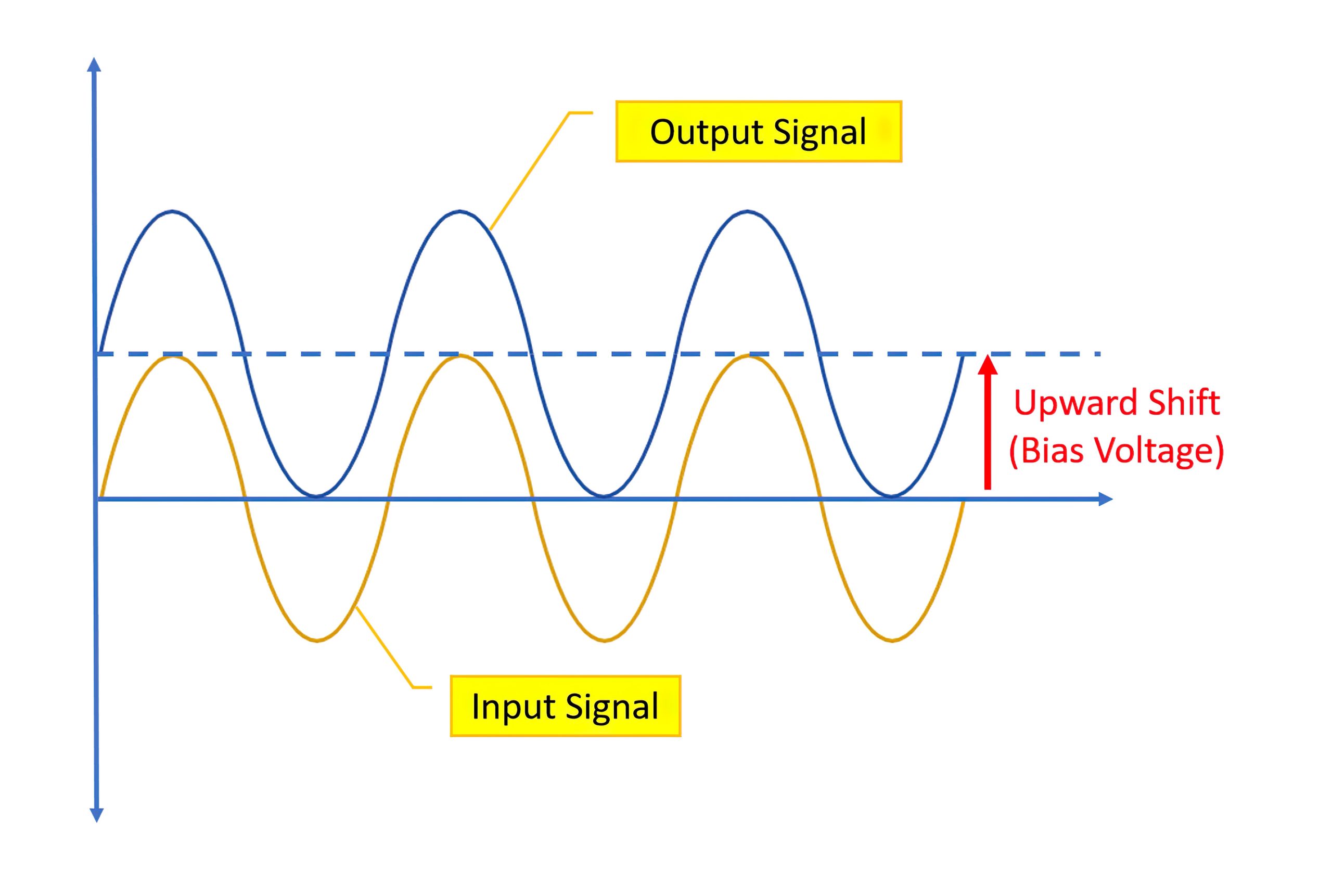
A clamper circuit shifts an input to a defined offset voltage by adding a variable positive or negative DC voltage to it; see Figure 1. The circuit will move the signal up or down, to position the peak at the reference level; see Figure 2. The input signal is shifted up by a predetermined magnitude, called “bias voltage”.
There are many types of clamping circuits; those that shift the input up are “positive-biased” clamper circuits, and those shifting it down are “negative-biased”. These circuits are also known as “DC voltage restorers”.
Clamper circuits are found in many applications, but are mainly used as voltage multipliers or to remove input signal distortions.
Here, we will determine how their DC shift voltage is affected by a changing input frequency. This is an important question since some clamping circuits are designed specifically to handle a range of input signal frequencies. Circuit performance and stability as frequencies change will impact the final design.
We will also examine the circuit’s behaviour at various bias voltage source values (V2).
Experiment setup
For the experiment we use a typical op-amp-based clamper circuit, as shown in Figure 1, which uses a general-purpose op-amp, LF351, and diode 1N914.
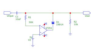
Figure 1: A typical op-amp-based clamper circuit

Figure 2: Clamper circuit input vs output
Throughout the experiment we fed a sinusoidal signal into the clamper circuit, with a changing frequency from 1Hz to 100kHz, yet keeping the bias voltage source (V2) the same. To evaluate the circuit’s performance, the amplitude of the upward shift in the input signal is evaluated at each frequency step during circuit operation. To obtain a complete spectrum of the circuit performance chart, the same operations were done for various bias voltage sources (V2).
Then we monitor two parameters as follows:
- The upper shifts that occur to the input signal at various frequencies and various bias voltage sources (V2); and
- The output signal’s peak-to-peak values at various frequencies and bias voltage source (V2).
The data was then plotted to determine the relationship between these parameters.
For the experiment we assumed the following:
- We kept the input signal magnitude fixed at 5V (peak-to-peak).
- All circuit component values were kept unchanged, except the bias voltage (V2), which varied from 1Vdc to 5Vdc, at 1Vdc increments.
- The temperature was kept at ambient 25o
The impact of frequency on circuit performance
Figure 3 shows the relationship between the applied frequencies, the bias voltage (V2) and the upward shift voltage. It can be seen that the circuit delivers a consistent and dependable performance over the whole frequency range from 1Hz to100kHz, correctly shifting the input signal by the same magnitude for each bias voltage, V2. This shows that the clipper circuit offers a satisfactory frequency-linked performance.
Figure 3: Relation between the input and output voltages during input frequency changes
The impact of bias voltage on circuit performance
The experiment also showed a connection between the bias voltage and the peak-to-peak amplitude of the output signal for a wide range of input frequencies. Figure 4 shows that the circuit can maintain a peak-to-peak signal output that is quite steady for signal frequencies above 11kHz. However, the output signal’s peak-to-peak magnitude is significantly distorted for frequencies below 11kHz. In addition, there’s a degree of distortion proportional to the level of bias voltage.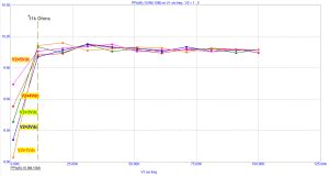
Figure 4: Output signal peak-to-peak magnitude at various frequencies and bias voltages
We can conclude that the clamper circuit offers a steady performance for different input signal frequencies, especially between 1Hz and 100kHz. However, that peak-to-peak value of the output signal is only maintained for input frequencies greater than 11kHz, but not for those below 11kHz – where the generated signal is quite distorted. The output signal will exhibit a greater degree of distortion in proportion to the degree to which the bias voltage level is reduced.
These results allow circuit designers to compensate for the clamper circuits in different applications, and thoroughly test their circuit for the targeted frequencies.
By Dr Sulaiman Algharbi Alsayed, Managing Director, Smart PCB Solutions