The Sallen-Key low-pass filter is one of the most popular second-order active low-pass filters, with a design similar to that of a voltage-controlled voltage-source (VCVS), with filter characteristics including high input impedance, low output impedance and good stability.
The circuit consists of one op-amp, a couple of resistors and a couple of capacitors; see Figure 1. Despite its simple design, its efficiency is quite high, with a sharp drop in output signal amplitude when a high frequency signal is applied to the input.
At first glance its frequency performance appears smooth, but we must check if there are any DC-offset components at the output that need to be compensated for with a DC-offset circuit. This is an essential point any circuit designer should verify before finalising a design.
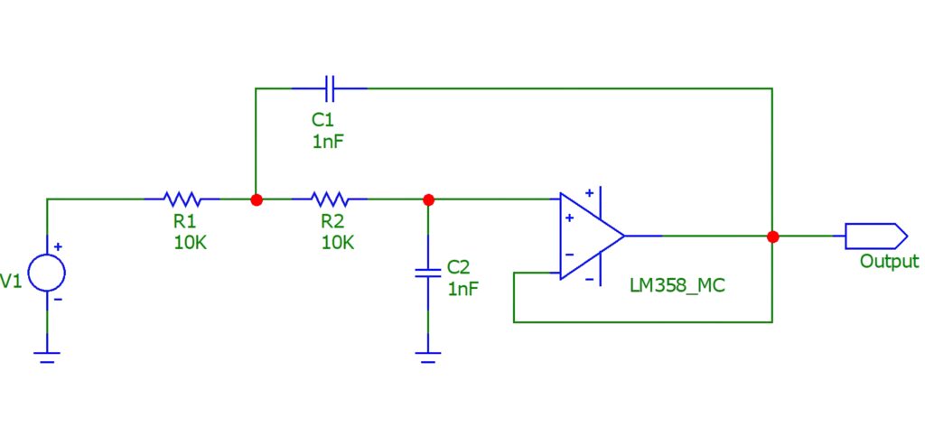
Figure 1: Sallen-Key low-pass filter

Figure 2: Output signal’s magnitude vs. input signal frequency in Sallen-Key low-pass filter
Experiment setup
We connect the low-pass filter to a function generator that generates a sinusoidal signal with frequencies from 1Hz to 100kHz (no need to go any higher for this circuit). The input signal’s frequency was applied gradually, at fixed intervals. We also assumed the following:
- The input signal amplitude was kept constant at 5Vac throughout the experiment.
- R1, R2, C1, C2 and the op-amp were kept unchanged.
- The voltage power supply was kept constant to avoid interfering with the collected data.
- The circuit output was not connected to any load.
The DC-offset voltage was measured and logged at each given input signal frequency. After a few milliseconds, when the signal stabilises, we measure the DC-offset voltage, which is then plotted against the varying input signal frequencies; see Figure 3.
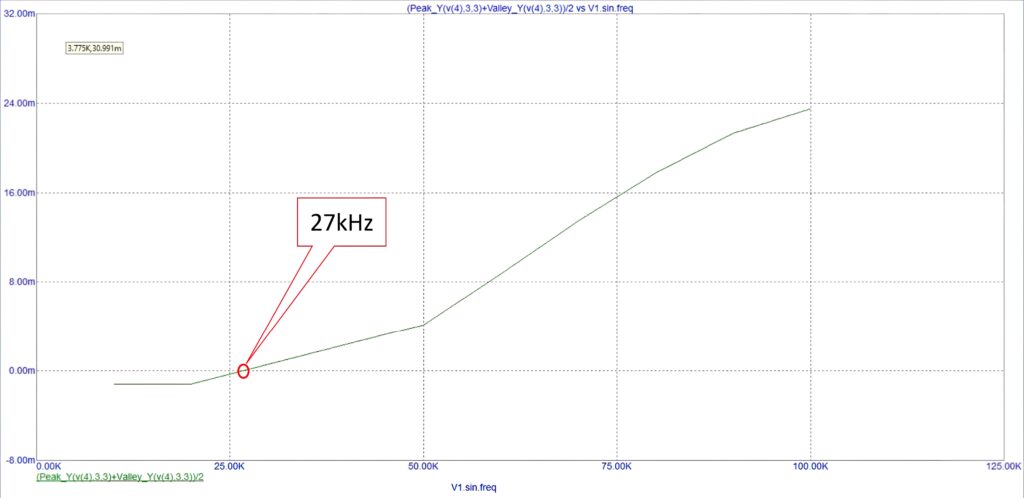
Figure 3: Output signal amplitude vs input signal frequency
The curve shows that the Sallen-Key low-pass filter circuit generates a DC-offset component at the output that can be damaging to any circuit connected to the filter. In Figure 3, the output signal DC-offset voltage is on the negative side for input frequencies below 27kHz, while it is positive when input frequencies are above that limit. This is an important finding and must be considered by circuit designers, since they must add a DC-offset circuit at the output of this filter to eliminate any potentially damaging DC-offset voltage components.
By Sulaiman Algharbi Alsayed, Managing Director, Smart PCB Solutions