Many setups require two or more power sources and there can be problems when switching between them. For example, almost all portable electronic devices have integrated rechargeable batteries and a USB port for charging. This requires a solution for seamlessly transitioning between the internal battery and the external power sources. But, connecting multiple power supplies to a single input without any protection can result in loss of power, power failure and short circuits. For that, power multiplexer (power MUX) devices are used as a reliable solution.
In this article we will discuss the manual switching between two power sources using the Renesas SLG59H1405V high-voltage GreenFET load switch.
The power MUX concept
Power multiplexers provide a seamless transition between two or more power inputs, and are typically used in computers, digital cameras, modems, cellphones and others, but also in battery management and peripheral power interface systems.
Generally the power MUX device switches between two input power supplies to one common output supply rail and thus provides a continuous supply for the system; see Figure 1, which shows a simplified block diagram of a power MUX.

Figure 1: power MUX simplified block diagram
The power MUX is typically implemented by controlling MOSFETs’ RDSON resistance because MOSFETs have high OFF isolation, which is important to prevent back-feeding power between two inputs.
From the control aspect, the output power rail can be chosen manually.
A manual power MUX is a device where each path is individually controlled by an external signal (logic or microcontroller). Figure 2 shows an example of a manual power MUX with two enable inputs. This method is generally used when there is a microcontroller that decides under what conditions to enable each input.

SLG59H1405 details
The Renesas SLG59H1405V device is suitable for power MUX applications. It comes with one 5V, 3A and one 12V, 1.25A-rated load switch with common output. The part allows manual selection and seamless transition between available inputs, and it provides several protection features.
The part is designed for typical 5V/12V manual switchover power MUX applications, suitable for systems with multiple power sources. See the SLG59H1405V pin configurations in Figure 3.

Figure 3: Pin configuration for the SLG59H1405V
Each pin’s functions are as follows:
- GND: is the ground connection. Connect this pin to the system’s analogue or ground plane.
- VIN1: Input terminal of 5.5V-rated Channel 1.
- VIN2: Input terminal of 13.2V-rated Channel 2.
- VBUS: Output terminal of the SLG59H1405V power MUX.
- FLAG: An open-drain output, FLAG is asserted LOW when a VIN[1,2] overvoltage, undervoltage, current-limit, or an over-temperature condition is detected. Connect a 100kΩ external resistor from the FLAG pin to a local system logic supply. Connect to GND if not used.
- NC: No connect.
- EN1: EN1 turns on Channel 1 and is a low logic level CMOS input with EN1_VIL < 0.5V and EN1_VIH > 1.5V. While there is an internal pull-down circuit to GND (~ 1MΩ), connect this pin directly to the general-purpose output (GPO) of a microcontroller, application processor or system controller.
- EN2: This turns on Channel 2 and is a low logic level CMOS input with EN2_VIL < 0.5V and EN2_VIH > 1.5V. While there is an internal pull-down circuit to GND (~ 1MΩ), connect this pin directly to the GPO of a microcontroller, application processor or system controller.
- ILIM1: A 1%-tolerance, metal-film resistor sets the active current limit for Channel 1. A 20kΩ resistor sets the active current limit to 4.01A.
- ILIM2: A 1%-tolerance, metal-film resistor sets the active current limit for Channel 2. A 20kΩ resistor sets the active current limit to 1.94A.
The SLG59H1405V in power MUX applications
Using the SLG59H1405V in manual power rail selection applications requires an external voltage VEN[1,2] > EN[1,2]_VIH to be applied to the EN[1,2] pins, which are typically connected to the MCU or other logic-level source.
To turn on one of the channels, both VIN1 and VIN2 voltages should be within the operating voltage range (VIN[1,2] > VIN[1,2]_UVLO and VIN[1,2] < VIN[1,2]_OVP), otherwise the part will latch off and EN1 and EN2 signals will be ignored. When a logic high (VEN[1,2] > EN[1,2]_VIH) is applied to the EN[1,2] pin, Channel 1 or Channel 2 will be on output, respectively. Note that to turn on Channel 2 in the SLG59H1405V, EN2 > EN2_VIH should not be applied sooner than 100ms after EN1 > EN1_VIH, otherwise the EN2 signal will be ignored and the switchover to Channel 2 will not be possible until EN1 < EN1_VIL and then EN1 > EN1_VIH again. Basically, to turn on Channel 2, Channel 1 should always be turned on first.
The FLAG pin can be pulled high with a resistor to provide feedback on the system’s status. FLAG is asserted LOW when a VIN[1,2] overvoltage, undervoltage, current-limit or over-temperature condition is detected. Connect to GND if not used.
Figures 4-8 show the turn-on, turn-off and switchover behaviour of the SLG59H1405V for VIN1 = 5V and VIN2 = 12V. The current limit is set at 4A for Channel 1 and 1.9A for Channel 2. Figure 4 shows a typical connection diagram for these conditions.

Figure 4: Connection diagram of using the SLG59H1405V in power MUX applications for VIN1 = 5V and VIN2 = 12V
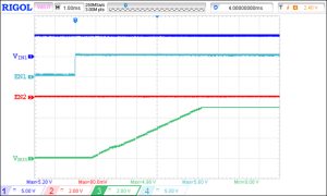
Figure 5: Turn-on operation waveform of the SLG59H1405V for VIN1 = 5V and VIN2 = 12V, EN1 = Low -> High, EN2 = Low, RLOAD = 5Ω, CLOAD = 20μF
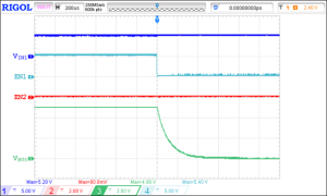
Figure 6: Turn-off operation waveform of the SLG59H1405V for VIN1 = 5V and VIN2 = 12V. EN1 = High -> Low, EN2 = Low, RLOAD = 5Ω, CLOAD = 20μF

Figure 7: Switchover operation waveform of the SLG59H1405V for VIN1 = 5V and VIN2 = 12V. EN1 = High, EN2 = Low -> High, RLOAD = 12Ω, CLOAD = 20μF

Figure 8: Switchover operation waveform of the SLG59H1405V for VIN1 = 5V and VIN2 = 12V. EN1 = High, EN2 = High -> Low, RLOAD = 12Ω, CLOAD = 20μF
SLG59H1405 protections
The SLG59H1405 load switch offers several protections, including over voltage (OVP), under-voltage lockout (UVLO), over current (OCP), short circuit (SCP) and over-temperature protection (OTP). Once one of these has triggered (except UVLO), the SLG59H1405 goes to latch-off. To release the part from this condition, both EN1 and EN2 must be set lower than EN[1,2]_VIL.
Over voltage protection
Тhe OVP is always monitoring the input voltage, regardless of which channel is active. Once VIN1 > VIN1_OVP or VIN2 > VIN2_OVP, the SLG59H1405V will latch off within a TOVP response time.
See its behaviour in Figures 9-14. The figures show the device’s recovery from latch-off for VIN1 = 5-6V and VIN2 = 12V. Figure 9 and Figure 10 show the device’s behaviour when Channel 1 is active, and Figure 11 when Channel 2 is active. A typical connection diagram for these conditions is shown in Figure 4.

Figure 9: The waveform of OVP behaviour and recovery from latch-off for Channel 1 for VIN1 = 5-6V and VIN2 = 12V. EN1 = High, EN2 = Low, RLOAD = 100Ω, CLOAD = 2.2μF

Figure 10: OVP behaviour and recovery from latch-off waveform for Channel 1 for VIN1 = 5-6V and VIN2 = 12V. EN1 = High, EN2 = Low, RLOAD = 100Ω, CLOAD = 2.2μF (extended view)

Figure 11: OVP behaviour and recovery from latch-off for Channel 1 of for VIN1 = 5-6V and VIN2 = 12V. EN1 = High, EN2 = High, RLOAD = 100Ω, CLOAD = 2.2μF
Figures 12-14 show SLG59H1405V’s OVP latch-off behaviour and recovery for VIN1 = 5V and VIN2 = 12-15V. Figure 12 shows the waveforms when Channel 1 is active, and Figures 13-14 when Channel 2 is active. The connection diagram for these conditions is shown in Figure 4.

Figure 12: OVP behaviour and recovery from latch-off for Channel 2 for VIN1 = 5V, VIN2 = 12-15V. EN1 = High, EN2 = Low, RLOAD = 100Ω, CLOAD = 2.2μF

Figure 13: OVP behaviour and recovery from latch-off for Channel 2 for VIN1 = 5V, VIN2 = 12-15V. EN1 = High, EN2 = High, RLOAD = 100Ω, CLOAD = 2.2μF

Figure 14: OVP behaviour and recovery from latch-off for Channel 2 for VIN1 = 5V and VIN2 = 12-15V. EN1 = High, EN2 = High, RLOAD = 100Ω, CLOAD = 2.2μF (extended view)
Under-voltage lockout
The UVLO is always monitoring the input voltage, regardless of which channel is active. Once VIN1 < VIN1_UVLO – VIN1_UVLO_HYS or VIN2 < VIN2_UVLO – VIN2_UVLO_HYS SLG59H1405V turns off. To recover to normal operation, both VIN[1,2] should be higher than VIN[1,2]_UVLO.
Figures 15-16 show the SLG59H1405V’s UVLO behaviour for VIN1 = 5-3V (notice the step-down) and VIN2 = 12V. A typical connection diagram for these conditions is shown in Figure 4.
Figure 15 shows the UVLO behaviour when Channel 2 is selected. If this sequence is not followed, Channel 2 will be disabled, signals on EN2 will be ignored and only Channel 1 will be active; see Figure 16.

Figure 15: UVLO behaviour and recovery for Channel 1 for VIN1 = 5-3V and VIN2 = 12 V. EN1 = High, EN2 = High -> Low -> High, RLOAD = 100Ω, CLOAD = 2.2μF
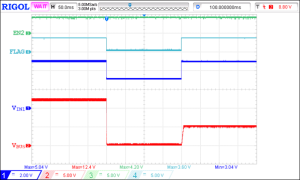
Figure 16: UVLO behaviour for Channel 1 for VIN1 = 5-3V and VIN2 = 12V. EN1 = High, EN2 = High, RLOAD = 100Ω, CLOAD = 2.2μF
Over current protection
OCP is designed to protect the entire device from excessive current damage, significantly increasing the fault tolerance of the entire device.
The output current is initially limited to the Active Current Limit specification given in Table 1.
The current-limiting circuit is very fast and responds within a few microseconds to sudden loads. When an overload is sensed, the current-limiting circuit increases the FET resistance to keep the current from exceeding the active current limit (ACL) for TOCP_delay and, then, if the overcurrent condition persists, the SLG59H1405V is latched-off. To release the part from latch-off state, both EN[1,2] must be lower than EN[1,2]_VIL.
The ACL level can be adjusted by choosing the appropriate ±1%-tolerance RILIM1 resistor value for Channel 1 and RILIM2 resistor value for Channel 2, and can be calculated by the following equations:
For RILIM1 ranging from 160kΩ to 20kΩ and for RILIM2 ranging from 75kΩ to 20kΩ

where:
RILIM[1,2] = Resistor on ILIM[1,2] pins, in kOhms (Ω).
Please note that if RILIM[1,2] > 600 kΩ, ILIM[1,2] pin is open, RILIM[1,2] < 2 kΩ or ILIM[1,2] pin is shorted to GND the ACL threshold will be IACL_VIN[1,2] = 0.5 A.
| RILIM1, (kΩ) | IACL_VIN1 (A) | RILIM2, (kΩ) | IACL_VIN2 (A) |
| 600 | 0.5 | 600 | 0.5 |
| 160 | 0.65 | 75 | 0.47 |
| 130 | 0.78 | 56 | 0.65 |
| 80 | 1.19 | 40 | 0.93 |
| 40 | 2.19 | 27 | 1.41 |
| 27 | 3.08 | 20 | 1.94 |
| 20 | 4.01 | 2 | 0.5 |
| 2 | 0.5 | ||
Table 1: Setting the current limit level vs. RILIM[1,2]
During an active current limiting operation, the die temperature rises due to the increased FET resistance. If the die temperature exceeds the THERMON specification, the SLG59H1405V will also latch off. To release the part from this state, both EN[1,2] must be lower than EN[1,2]_VIL.
Figure 18 shows the SLG59H1405V’s overcurrent protection behaviour for Channel 1 for VIN1 = 5V, VIN2 = 12V, with a step load RLOAD = 1Ω. The connection diagram is shown in Figure 17.

Figure 17: Connection diagram of using the SLG59H1405V in power MUX applications during OCP for VIN1 = 5V and VIN2 = 12V
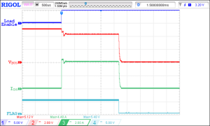
Figure 18: OCP behaviour for SLG59H1405V’s Channel 1 for VIN1 = 5V and VIN2 = 12V. EN1 = High, EN2 = Low, RLOAD = 1Ω, CLOAD = 20μF
Short-circuit protection
SCP protects the entire device from damage caused by high short-circuit currents. A short circuit can occur as a result of the failure of the connected device or from a mechanical impact. Such protection significantly increases the fault tolerance of the entire device.
Once output IVBUS current will hit the short-circuit protection threshold (ISCP), the SLG59H1405V immediately shuts down, and then repowers with lower current limit threshold that can be calculated by the following equation:
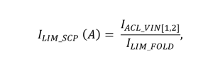
where:
ILIM_SCP = VBUS current limit after triggering VBUS short circuit protection
IACL_VIN[1,2] = active current limit threshold set by RILIM[1,2]
This re-powerup will last during TOCP_delay and then SLG59H1405V latches off. To release the part from latch-off, both EN[1,2] must be lower than EN[1,2]_VIL.
Figures 20-21 show the SLG59H1405V’s SCP behaviour for Channel 1 for VIN1 = 5V and VIN2 = 12 V, with a step load RSHORT = 0.5Ω. A typical connection diagram for these conditions is shown in Figure 19.
For Channel 2, the SCP shows the same behaviour with a corresponding ILIM_SCP current.
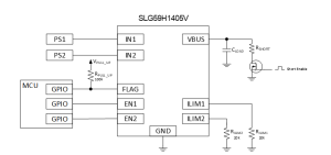
Figure 19: Connection diagram of using the SLG59H1405V in PowerMUX applications during SCP for VIN1 = 5V and VIN2 = 12V

Figure 20: SCP behaviour for SLG59H1405V’s Channel 1 for VIN1 = 5V and VIN2 = 12V. EN1 = High, EN2 = Low, RSHORT = 0.5Ω, CLOAD = 20μF
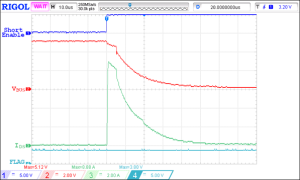
Figure 21: SLG59H1405V SCP behaviour for Channel 1 for VIN1 = 5V and VIN2 = 12V. EN1 = High, EN2 = Low, RSHORT = 0.5Ω, CLOAD = 20μF (extended view)
Indispensable
Power Mux is an indispensable device for applications that require several input power supplies with a common output load. Using the Renesas SLG59H1405V device, which was specially designed for power MUX applications, the process of controlling the switching between different power sources is easier and safer. With its extensive protection functionalities, it is ideal battery‑powered devices, USB ports and other low‑voltage applications, offering a simple and efficient way to control power the appliance.
By Yurii Makhovych, Junior App and Documentation Engineer, Renesas Electronics, Lviv, Ukraine