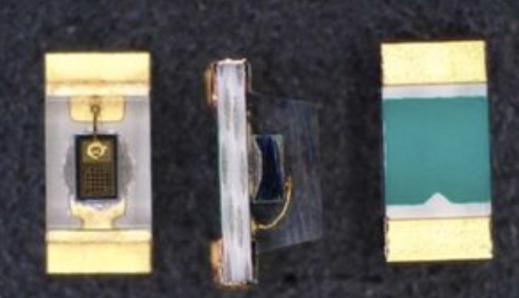
Marktech Optoelectronics and its manufacturing partner Optrans are introducing new transfer-moulded photodiode and LED packages, scheduled for Q2 2026. These next-generation photonics packages offer improved reliability, optical beam control, enhanced environmental robustness and reduced stray-light interference while supporting both conventional LED emitters and advanced point-source RCLED and QWLED architectures.
Transfer moulding forms a precision optical and mechanical structure directly over the die, encapsulating the LED or detector in a controlled moulding process that produces exceptional part-to-part uniformity, tighter beam profiles, stronger wire-bond protection, and improved long-term reliability under temperature and humidity stress. This approach offers significant advantages over traditional packaging methods — such as glob-top epoxy, liquid potting, COB silicone domes, and discrete lens cap assemblies — making it especially well-suited for industrial, medical, instrumentation, aerospace, and automotive applications that require repeatable performance, a small footprint for dense packing, and robust handling.
Engineering prototypes are planned for release in early 2026, with full production availability beginning in Q2 2026.
Transfer-moulded photodetector, and LED packages will be available in select JEDEC and IPC SMD footprints. Custom sizes and optical geometries can be developed to OEM design specifications. Additional potential photonics packaging variations include options for integrated lenses, phosphor layers, filter windows, and light shielding. Initially, chip sizes up to 350µm × 350µm can be packaged. Marktech’s new transfer-moulded packaging is suitable for emission and detection from 355-230nm.