You often work with transmit – receive systems where the transmitter dominates the bill of materials, board area, and power budget, and this is just as true for infrared (IR) links as for RF links. In your IR designs, improving the front‑end receiver sensitivity lets you either push the operating range further out or dial back laser power for the same range, so you constantly balance these two levers during system design.
When you build a time‑of‑flight or distance‑measurement setup, LiDAR, laser rangefinder, or benchtop optical tester, you typically fire short, high‑power pulses from a laser diode and then capture the returned light with one or more IR sensors at the receiver input. You care less about the absolute transmit power than about how effectively your detector can pull a tiny, reflected signal out of the noise, because that determines whether you can see a distant or low‑reflectivity target without oversizing the laser.
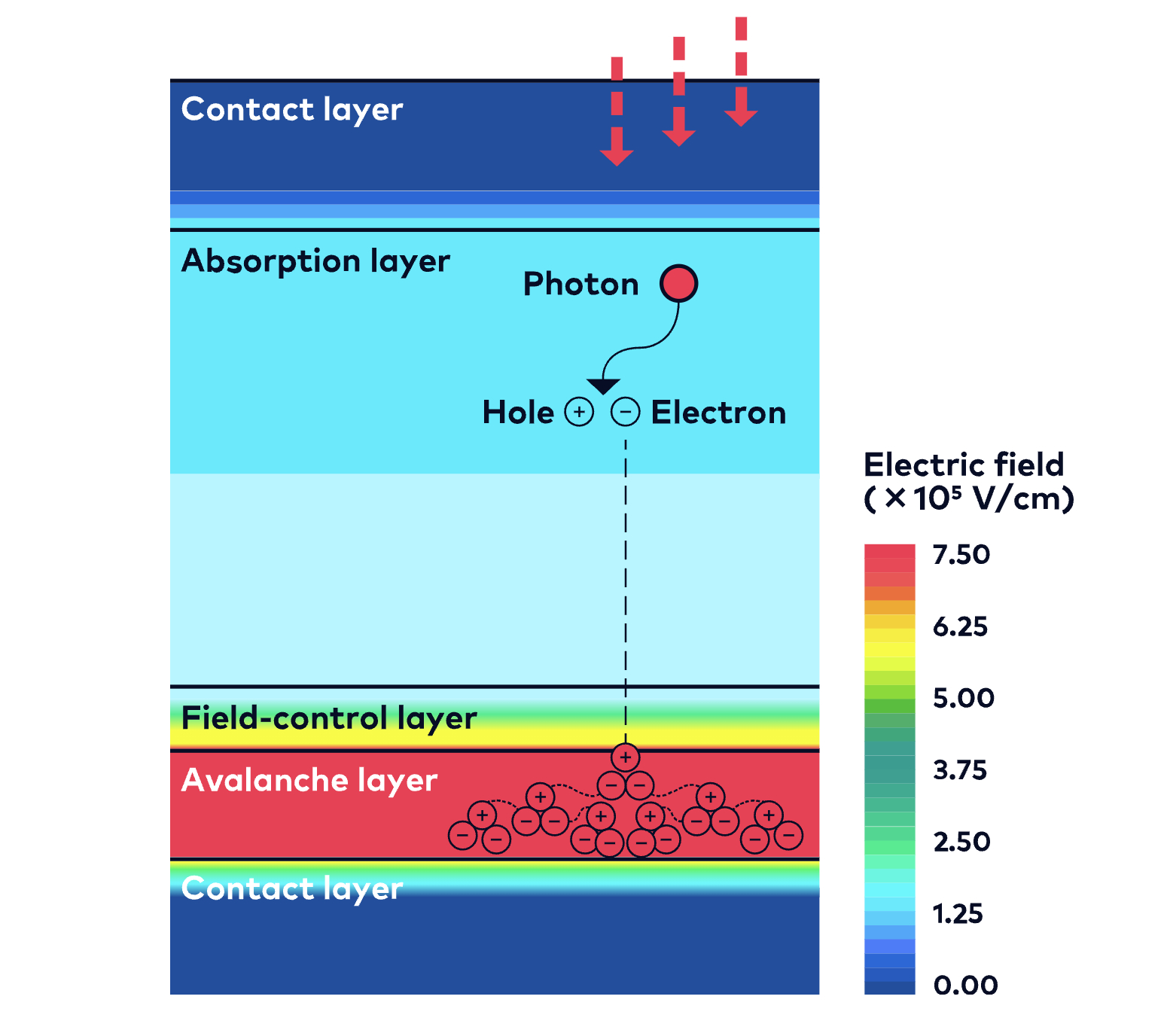
To reach the required sensitivity in the IR band, you frequently turn to avalanche photodiodes (APDs) as your detector of choice. Inside each APD, a carefully engineered semiconductor layer converts incoming photons into electrical current by generating electron‑hole pairs, and the device structure steers these charge carriers to opposite electrodes under an applied electric field.
As you increase the reverse‑bias voltage, the APD enters its avalanche region, where the internal field becomes strong enough that carriers pick up enough energy to ionize additional atoms and create more carriers. This internal multiplication gives you current gain directly inside the sensor, so a handful of photons can produce a measurable output pulse, and in optimized devices a single photon can be enough to trigger a detectable event.

Reverse‑biased avalanche photodiode structure showing internal gain from impact ionization.
You set an APD’s usable wavelength range primarily by the semiconductor material you choose for the device. When you pick silicon, you target a peak response around 900 nm and you can usually run with internal avalanche gain from roughly 50 up to about 1,000.
If you instead choose germanium or indium gallium arsenide (InGaAs), you push your sensitivity out to longer wavelengths, roughly 1000 to 1700 nm. In these materials, you typically work with more modest avalanche gains in the order of 10 to 40, because higher gain brings a significant noise penalty in compound semiconductors, with InGaAs generally giving you a lower‑noise option than pure germanium for the same range.

Typical wavelength response and gain ranges for silicon, Ge, and InGaAs avalanche photodiodes.
You pay a premium for InGaAs APDs because they use a compound semiconductor process, so device cost comes out higher than for silicon parts. Given those constraints, you only choose an InGaAs APD when the operating wavelength really matters.
When you design with silicon APDs, you are working near 905 nm, close to the visible region of the spectrum. At this wavelength, IR light that reaches the eye can damage the retina, so safety rules force you to cap laser diode output power, and that cap directly limits how far a silicon‑based system can reach.
If you instead specify InGaAs APDs, you move into the 1300 nm to 1550 nm window, with 1550 nm being especially common in practice. In this so‑called eye‑safe band, you can drive IR lasers to powers that are hundreds of times higher yet still comply with safety limits, which lets you extend operating distance without putting users’ eyesight at risk.
For years, one of your main design headaches with InGaAs APDs has been the extra noise created by the avalanche multiplication process, which cuts sensitivity. Newer structures that incorporate antimony into the compound semiconductor stack have begun to overcome this, cutting avalanche noise and delivering several other performance gains at the same time.
Reducing Avalanche Noise with Antimony‑Enhanced InGaAs APDs
In a conventional APD, the avalanche multiplication you rely on for gain also generates a lot of noise, and that directly undercuts sensitivity. The usual multiplication‑layer materials let impact ionization create holes and electrons with similar probability, and the strong internal field then accelerates positive and negative carriers in opposite directions, so each injected carrier can trigger a very different chain reaction.
Because the process is so random, one event can run away and multiply for a long time, while the next may produce very little gain at all. Once you push the device to higher reverse bias, this statistical spread takes over, so beyond roughly a gain of 10 to 20 the noise from the avalanche process starts to dominate the signal you care about.
In the newer InGaAs APD design, you switch to a multiplication layer made from a semiconductor alloy that includes antimony. In this material, virtually every impact ionization event generates electrons, and the avalanche action is confined to a well‑defined region inside the multiplication layer, which gives you a far more controlled response.
Because that alloy layer is homogeneous and compatible with standard processing, you can build the device repeatably while benefiting from an almost deterministic gain mechanism. The excess noise drops enough that you can safely operate at avalanche gains up to about 120 without the multiplication noise swamping your signal.
On top of this, you must still fight the baseline noise from thermally generated carriers, the dark current that flows even with no light present. By tightening up process conditions, refining the device structure, and improving material purity, the dark current in the latest “Aura” Noiseless InGaAs APD generation has been cut by more than three‑quarters compared with earlier versions.
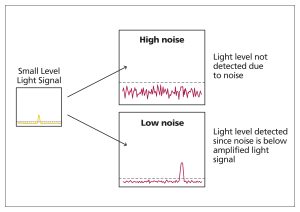
Aura InGaAs APD architecture reduces dark current, improving signal‑to‑noise ratio.
When you combine very low excess noise with very low dark current in a single device, you end up with a commercial APD that delivers roughly a twelve‑fold increase in sensitivity over earlier high‑end parts. That gain in sensitivity lets you design time‑of‑flight systems that are smaller, more power‑efficient, and more affordable to build.
At the same time, the improved device structure gives you better long‑term stability, stronger overall performance, and higher robustness in demanding operating conditions.
Stable Gain and Wide Temperature Range with Aura InGaAs APDs
The low noise you get from the Aura APD helps keep its gain stable across normal operating conditions. With traditional APDs, you must bias the device very close to breakdown to achieve high gain, so even small ripples or spikes on the supply can translate into large output swings, which makes these parts awkward to tame in a real design.
With Aura, you can bias the device further away from the breakdown point, so it is inherently easier to drop into your receiver front end. The same characteristic also makes the device less sensitive to temperature changes, a major headache when you run conventional APDs near breakdown, because breakdown voltage shifts directly with junction temperature.
In a typical system, even modest temperature shifts can move the breakdown point by hundreds of millivolts, yet you usually cannot measure the die temperature accurately or tweak the supply voltage on the fly. That is why conventional solutions often need extra compensation circuitry, which adds cost and board area, just to hold the gain roughly constant.
By contrast, you can run the Aura device safely away from breakdown and benefit from a much lower temperature coefficient, about 20 mV per kelvin for the breakdown voltage. That figure is up to an order of magnitude lower than in many legacy APDs, and, combined with the low dark current and excess‑noise performance, it lets you operate over a much wider ambient‑temperature range without elaborate thermal management.
For time‑of‑flight optics, you also need the APD to survive and correctly measure signals that range from a handful of photons to very strong reflections. In an automotive LiDAR scene, you might be reading a weak return from a distant black tyre one moment and a powerful flash from a nearby reflective number plate the next, so the detector has to cope with that extreme dynamic range without damage.
Tests on Aura devices show that they keep working even after repeated exposure to infrared pulses with intensities up to about 40 MW/cm². High optical loads can also slow down recovery from saturation, but you can minimise that effect by carefully matching the APD to its transimpedance amplifier, so the photodiode current is converted efficiently into voltage.
Using this approach, a prototype receiver module with Aura running at a gain of 10 recovers from a 500 kW/cm² overload in under 1.5 microseconds. When you increase the gain to 100, the overload recovery time for the same optical hit is still only about 2.5 microseconds, so the detector is ready quickly for the next return pulse.
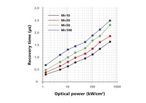
Fast APD recovery after high‑power pulses enables accurate detection of closely spaced return signals.
Co-designing the APD and TIA also makes it easier to pinpoint the arrival time of each incoming signal, which in turn improves the precision of the distance measurements. Accurate timing requires the signal response to have a rapid rise time and an equally fast decay time, and the prototype module demonstrated that it can distinguish between pulses arriving just 10 ns apart.
Summary
By bringing together high sensitivity, low noise, and carefully tuned behaviour for speed, impulse response, overload recovery, and high‑temperature operation, Aura APDs give you a single device that fits a wide range of infrared system roles. In many existing designs, you can drop them into slots currently occupied by standard InGaAs APDs and see an immediate uplift in performance without major hardware changes.
When you design a new IR system, that extra sensitivity lets you switch to far cheaper solid‑state lasers and still hit your range and accuracy targets, which cuts size, bill‑of‑materials cost, and overall system complexity. Depending on what your application values most, you can instead trade the sensitivity margin for higher measurement speed, reliable operation at elevated temperatures, or a significant extension in usable range, in some cases by as much as fifty percent.
By Phlux Technology CEO and Co-Founder, Ben White