One of the main purposes of using a composite configuration amplifier is to improve circuit performance against the DC voltage components that may combine with the AC input signal. This type of amplifier shows great stability of output signals when the AC input signal is mixed with a noisy DC component.
The circuit in Figure 1 shows a simple composite amplifier that works to 300MHz. I tested the circuit at a DC offset voltage of 1-15V DC in combination with an input AC signal and found it very stable. The circuit continues to provide stable output regardless of the input DC offset voltage, which is great.
The next step was to check the circuit’s capability to handle a low output resistance load. I tried to identify the lowest connected output load resistance that can take the circuit out of its nominal performance. This would help me determine if the circuit remains stable at extremely low resistance loads.
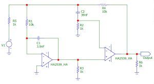
Figure 1: A typical composite amplifier circuit

Figure 2: The circuit’s output at 1Vdc and 40MHz
The experiment
For simplicity I used the circuit of Figure 1 for the experiment, although many other types of composite amplifiers exist. A range of output resistance was connected to its output, and its output signal peak-to-peak voltage measured, which was then plotted against each output load resistance value.
All electronic components were kept fixed throughout the experiment, except for output resistor, R6. The power supply for the op-amp HA-2539 was kept at ±15V DC. The input signal’s frequency was fixed at 40kHz, a value that was selected after noticing the circuit’s stable performance. The op-amp HA-2539 has a wide frequency bandwidth and the input signal amplitude was fixed at 1V DC.
During the experiment, I changed the load resistances between 1Ω and 30Ω.
Results
The results of the experiment are shown in Figure 3. It can be seen that the circuit exhibits great stability even at varying output load resistances. A discernible decline in the output signal’s peak-to-peak value is only noted when the output load resistance drops below the threshold of 2Ω.

Figure 3: Output signal peak-to-peak voltage vs. load resistance
This means that this circuit shows great stability across a wide range of output load resistances. This is a positive finding for circuit designers, who should note this circuit’s slight limitation when connected to low-resistance loads.
Furthermore, it is worth noting that the circuit’s stability under varying load conditions highlights its reliability and suitability for a wide array of applications.