CEA-Leti has fabricated a new gate-all-around (GAA) nanosheet device as an alternative to FinFET technology targeting high-performance computing (HPC) for smartphones, laptops and mobile systems with data collection and processing involving low-power and high-speed operation.
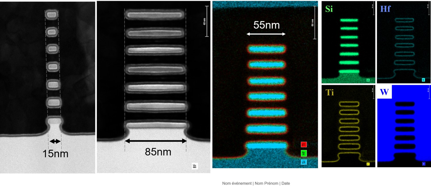
The GAA nanosheet transistors are fabricated with seven levels of stacked silicon channels, double that of state-of-the-art technologies today; widths range from 15nm to 85nm. The GAA transistors were fabricated using a replacement metal gate process, inner spacer and self-aligned contacts. CEA-Leti scientist Sylvain Barraud said the transistors’ gates can be controlled accurately and easily, with extremely high current drivability (3mA/μm at VDD = 1V), and a three-fold improvement in drain current over the usual two-level, stacked, nanosheet GAA transistors.
“By increasing the number of stacked channels, we increase the effective width of the device for a given footprint,” said Barraud. “Increasing the effective width induces higher drive current. This is why the DC performance of our devices is better than leading-edge devices.”
Barraud said CEA-Leti’s demonstration was based on a replacement metal-gate process developed for FinFET.
“We added specific modules for GAA structures on this FinFET route and we showed that for the same surface occupation we can propose an alternative to FinFET technology due to a gate-all-around configuration. GAA structures offer many advantages over FinFET, such as better gate control and higher DC performance, thanks to higher effective channel width. In addition, the wide range of variable nanosheet widths allows more design flexibility, which is not possible for FinFET because of its discrete number of fins.”