The Microtest Group, a manufacturer of test systems and testing of chips on packages and silicon wafers, has launched two turnkey platforms for power device characterization: Quasar200and Pulsar600. These systems mark a significant advancement in WBG semiconductor research and product development, especially in the automotive sector.
Developed by ipTEST, Microtest’s UK subsidiary and a global leader in high-volume power semiconductor testing systems, the two platforms set a new benchmark in precision testing. They assess the ability of devices to handle high currents and voltages safely and efficiently.
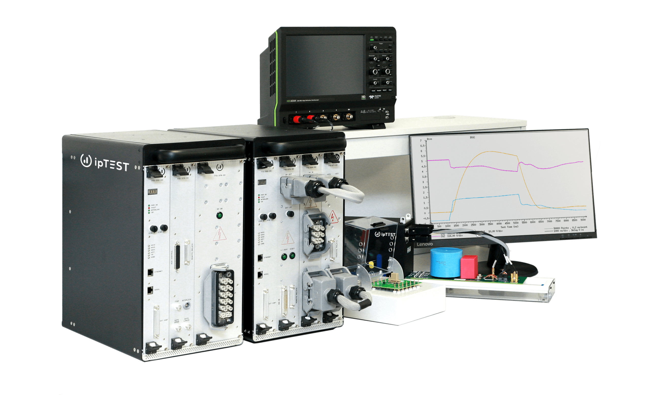
Quasar200and Pulsar600 are designed for two key communities in the sector: academic researchers and engineers developing new semiconductor products. With a plug-and-play approach, they simplify experimental workflows by eliminating the need for custom equipment and reducing manual operations such as soldering and complex test setups. This enables users to obtain accurate, publication-ready results with traceable precision. Their reliability speeds up datasheet generation, facilitates correlation with production testers, and ensures safe validation of next-generation devices.
Quasar200 is suitable for evaluating Si (silicon), GaN (gallium nitride), and SiC (silicon carbide) devices. It delivers fast and accurate DC/AC measurements with minimal parasitic inductance. Its counterpart, Pulsar600, extends these capabilities to ultra-high current applications, ideal for testing SiC inverters and automotive systems, supporting short-circuit tests up to 1,000 A DC and 10,000 A+ AC.
Both platforms offer up to ±0.1% measurement accuracy across all voltage and current waveforms, with typical parasitic inductance below 30 nH in AC tests. UKAS (United Kingdom Accreditation Service)-traceable calibration and comprehensive audit logs ensure reliability, consistency, and compliance from lab benches to production lines.
From a safety perspective, ipTEST’s SocketSafe technology and a fully enclosed test environment with interlocked access protect both operators and hardware – crucial during high-stress or destructive testing. This safeguards investments, maximizes uptime, and ensures peace of mind when pushing devices to their performance limits.
Finally, low-inductance test sockets – connectors designed to minimize inductance and avoid interference with critical measurements – and a modular design make it easy to evaluate and configure both packaged and bare die samples, streamlining setup and reducing complexity.