We stand on the threshold of a revolution in sensor technology. By the end of the decade, short-wave infrared (SWIR) sensing and imaging will be a common feature in many systems – from automotive, consumer and medical to industrial automation – significantly enhancing their capabilities.
It is expected that the market for SWIR sensing will explode in just five years, to about $2.9bn from $322m in 2022 – largely thanks to advances in infrared quantum dot (QD) technology. QDs are nanoscale semiconductors that absorb and emit light across the near-infrared (NIR) and SWIR spectrum. Commonly based on lead sulphide (PbS), they are fabricated with simple benchtop wet chemistry, allowing their large-scale production.
SWIR sensing alternatives
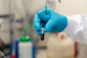
After years of intensive research, now QD technology is ready for commercial use in high-performance SWIR sensing.
QDs are a very exciting new technology for the industry because of the lack of alternatives suitable for widespread adoption. In terms of sensing capability, most other options on the market are missing certain critical functionalities or face other barriers for their use in consumer applications.
Silicon-germanium (SiGe) sensors are cheap but difficult to fabricate. Inherently they are low noise, easily meeting the signal-to-noise ratio required for most SWIR sensing and imaging applications. But, these sensors suffer from limited light detection ranges, peaking at around 1.4µm, which precludes them from being used in many SWIR applications.
In contrast, indium-gallium-arsenide (InGaAs) sensors operate within the SWIR region of 0.9-1.7µm, with high quantum efficiency, reliability, low dark current and fast response speed. Extended InGaAs sensors with higher indium arsenide composition can even detect wavelengths to 2.6µm.
The InGaAs technology is much more mature than SiGe, and is already used in machine-vision applications, defence and security. However, its primary downside is cost: Individual InGaAs units can cost up to $10,000, due in part to the high defect rates during their manufacture.
Creating an InGaAs sensor starts with epitaxially growing the material onto indium phosphide (InP) wafers. These wafers are then diced into chips, before pixels are indium-bonded with silicon readout circuits, through a process known as “flip-chip hybridisation”. This process leads to limited pixel pitch and resolution, as well as being complex and expensive to run. The result is a low-yield product that is highly susceptible to defect formation and is difficult to scale to larger wafer sizes because of the InP fragility. These systems also require significant cooling to achieve the desired image quality, which further increases the size of an already bulky product. All these problems make InGaAs sensors suited only for niche markets, where performance matters above cost and size.
If SWIR imaging and sensing are to become widespread in consumer electronics, engineers must look elsewhere for the solution.
QDs
QDs are already commonly used for display purposes since they can be tuned to emit visible light. However, their ability to be tuned to SWIR wavelengths is disrupting the industry by improving the quality and quantity of infrared data that can be accessed by all type devices.
During PbS QD formulation, directly controlling the size of the material enables the semiconductor band gap to be precisely tuned, with larger QDs sensitive to longer wavelengths of light, and smaller nanoparticles sensitive to shorter, higher-energy wavelengths – from 800nm to 2,400nm.
For optoelectronic applications, in addition to broadband tunability, QDs with a higher excitonic absorption peak and narrower full width at half maximum (FWHM) of the absorption spectrum offer superior performance. The capability to tightly control this specification is highly desirable in QD synthesis.
Quantum Science is a British expert in infrared QD technology. The company has already demonstrated industry-leading performance in this field by creating infrared PbS-based QDs that feature FWHM significantly better than market-available QDs. Using transmission electron microscopy to monitor the uniformity of shape and size distribution for QD materials shows that its INFIQ QDs are monodisperse, with diameters of 4.9 ± 0.1nm at 1,350nm and 6.0 ± 0.1nm at 1,550nm, respectively. Its QDs also feature high degree of crystallinity, meaning they experience a lower rate of defects and fewer electronic trap states, protecting them from performance degradation.
The QD ink formulation process
SWIR-sensitive QD films are typically created by exchanging the long-chain organic ligands (organic molecules that are optimised for synthetic control and colloidal stability) present on the surface. During this process, long-chain ligands are replaced with shorter, more conductive ones, making the resulting QDs suitable for use in optoelectronic devices.
By conducting the ligand exchange in solution, stable colloidal QD inks can be created. These inks overcome long-existing and key manufacturing challenges of QD sensor production where multi-steps spin coating methods are used.
The spin coating process sees up to 14 thin layers of QDs deposited sequentially, with chemical treatments applied to each layer and washing steps to replace the insulating ligands. This process very resource greedy, and the multi-layer deposition leads to high risks of defects occurring, with the end result being low-yield, higher-cost QDs and manufacturing.
In contrast, QD inks allow to deposit QD coatings in a single step, removing the need for further chemical processes and minimising defect occurrence. Additionally, it is significantly shorter and less labour intensive, enabling the mass production of high-performance optoelectronic devices and bringing SWIR sensing closer to market.
Applications
Infrared PbS QD technology has proven benefits for photodetection, photovoltaics and infrared light emitters. With reported photon conversion efficiencies of over 80% and granting outstanding SWIR sensitivity, infrared light from the sun is converted into energy, making these semiconductor materials revolutionising for most electronics-based systems. For product-sorting applications, QD-equipped SWIR sensors can detect specific spectral signatures, enabling them to monitor container fill levels or check for hidden spoilage, without causing unnecessary damage.
With SWIR light capable of peering deeper into tissue than any other wavelength, SWIR sensors can benefit medicine by detecting subdermal conditions even earlier.
In defence and security, QD-based scanning systems can better operate in all weather conditions because SWIR light is not scattered by dust or fog. For similar reasons, QD sensors can enhance vehicle Light Detection and Ranging (LiDAR) systems, increasing their effective range to 500m.
What’s more, with high-performance, lead-free QDs rapidly approaching market readiness, we will soon find SWIR-sensitive QDs in everyday consumer devices, dramatically improving the technologies we use every day.
As QD technology develops further, and as more electronics manufacturers learn of their benefits, this list of applications will grow, bringing the quantum revolution a lot closer.
By Dr Hao Pang, CEO and Founder, Quantum Science