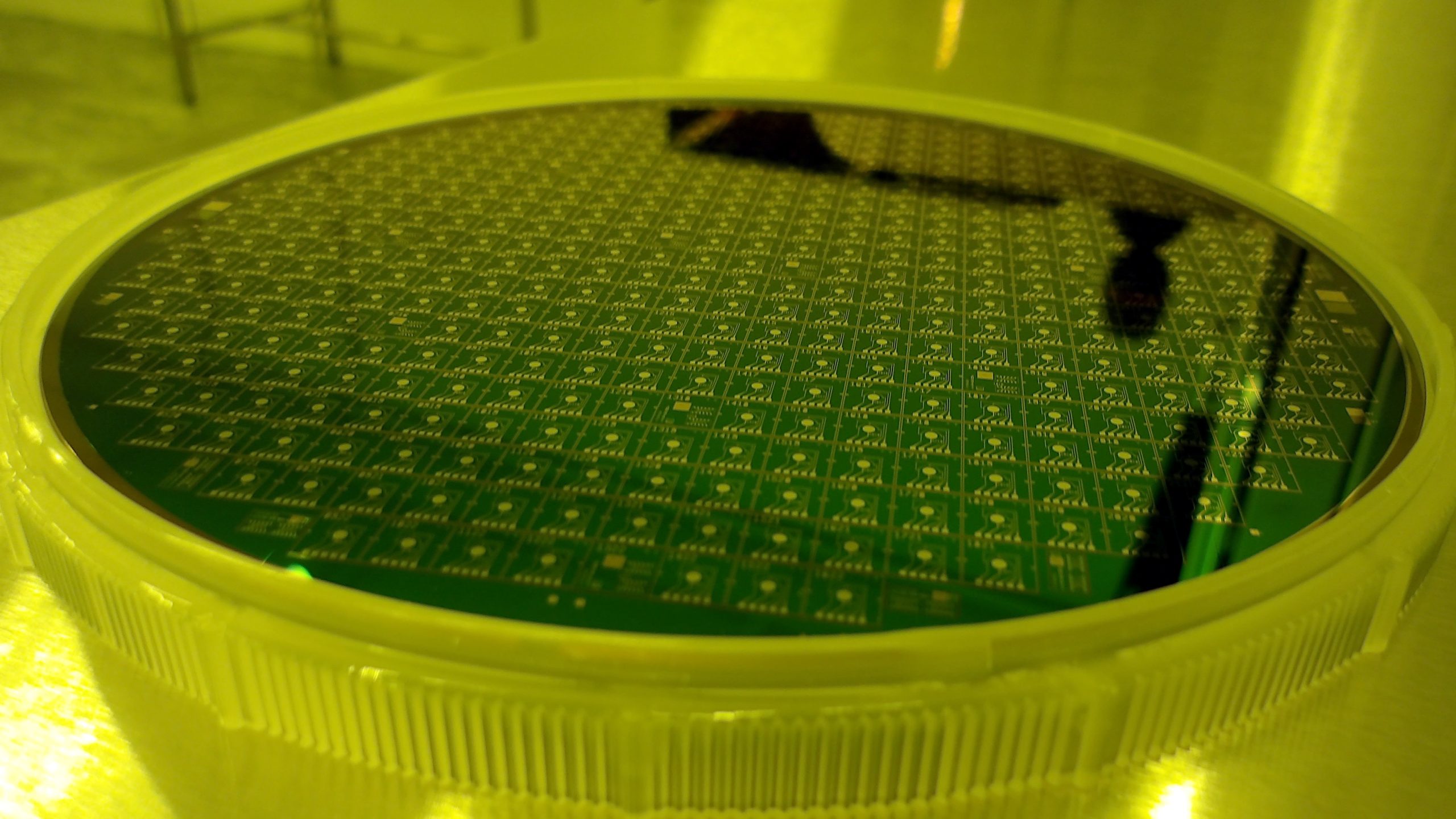
UK-based graphene company, Paragraf, has successfully produced its a 6-inch graphene wafer at its new manufacturing facility in Huntingdon, Cambridgeshire. The company is pioneering the commercialisation of graphene-based electronics using standard semiconductor processes.
“This first 6-inch wafer out of our Huntingdon facility is a landmark moment for Paragraf. It demonstrates both the maturity of our graphene growth technology and our ability to scale it on industry-relevant substrates, while maintaining the contamination-free advantages of our approach required by many applications and customers,” said Simon Thomas, Co-Founder and CEO of Paragraf.
The wafer contains graphene field-effect transistors (GFETs) fabricated using Paragraf’s proprietary process in which graphene is grown directly on silicon. This achievement represents a major step forward for scalable graphene electronics and is believed to be the first demonstration of GFETs on silicon using a direct-growth approach at this wafer size.
Until now, Paragraf has produced GFETs on 2-inch sapphire wafers using its contamination-free, transfer-free graphene growth technology. While other approaches to GFETs on silicon typically rely on transferring graphene from a growth substrate, often introducing metallic contamination, Paragraf’s direct-on-silicon process preserves material purity and device integrity while opening the door to greater compatibility with mainstream semiconductor manufacturing.
The transition from 2-inch to 6-inch wafers is a major milestone, enabling higher throughput, improved uniformity, and closer alignment with established semiconductor fabrication infrastructure. Together with the development to include silicon substrates, this positions Paragraf to accelerate the development of scalable graphene-based electronic and sensing devices.