The rapid growth of wireless technology is calling for reliable and high-performing communication systems. Here, filters play a crucial role, enabling the selection of desired signals. In particular, compact filter structures are essential, which in turn often require high dielectric constants to shrink their size. Thus, designing and developing efficient, compact RF filters has become a crucial effort.
From these, microstrip filters are favoured due to their light weight, small size, high efficiency and low cost. Microstrip bandpass filters are also easy to make, and provide reliable performance. They are designed to pass signals within a specific frequency range whilst attenuating those outside the desired bandwidth. Notably, open-loop resonators offer a simpler fabrication process compared to similar coupling geometries, such as waveguide cavity-coupled filters.
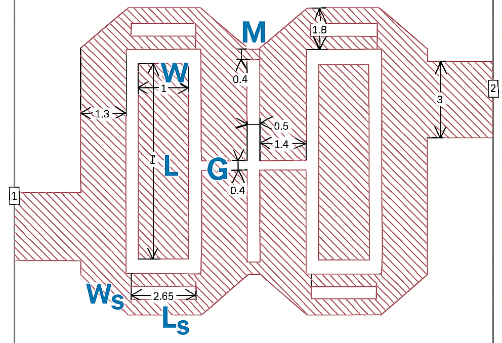
Harnessing the open-loop resonator geometry
Here we will discuss the design a microstrip bandpass filter utilising open-loop resonators, which demonstrate excellent performance in terms of bandwidth, selectivity and stopband attenuation, and allow filter size to be significantly reduced. However, a primary challenge lies in the small gaps within the resonator, which could lead to short-circuiting during manufacture. We used inductive and capacitive techniques to achieve a symmetric response across the passband.
The open-loop resonator exhibits unique electrical properties, making it ideal for bandpass filter applications. The square-shaped conductor loops are capacitively coupled to the microstrip transmission line, allowing for precise control of the frequency response by adjusting the resonator dimensions. A critical design consideration involves minimising passband loss whilst optimising the skirts of the rejection band to meet the desired design specifications, resulting in a symmetric and well-shaped passband.
Beyond their electrical performance, microstrip bandpass filters with square open-loop resonators offer additional benefits due to their planar structure, which facilitates compatibility with integrated circuit fabrication processes. Their small size and ease of manufacture make them ideal for applications like wireless sensor networks, mobile communication systems and microwave ICs. The quality factor of these filters is especially important in high-performance applications, such as satellite and fibre optic communications.
In the design of microstrip filters, various critical formulas play a significant role. The relevant equations used in this study include:
![]()
where Z0 is the characteristic impedance, is the relative permittivity of the used substrate, h is the substrate’s height, w is the width of the strip line and t is the thickness of the copper.

where is the effective dielectric constant, is the relative permittivity of the used substrate, H is the substrate’s height and W is the width of the strip line.

where is the resonance frequency, is the effective dielectric constant and L is the length of the strip line.

where BW is the bandwidth, is centre frequency and Q is the filter’s quality factor.
These expressions govern the characteristic impedance Z0, effective dielectric constant εeff , and resonant frequency fr. By fine-tuning the transmission line dimensions, we ensured optimal power transfer and effective coupling between the feedline and the resonator, thereby enhancing the filter’s overall performance. Special attention was given to the discontinuities introduced by the open-loop geometry, which are critical for achieving the desired coupling strength and filtering characteristics.
In this work, we extend conventional design techniques by incorporating a multi-objective optimisation strategy addressing electromagnetic field distribution, sensitivity to fabrication tolerances, and trade-offs between bandwidth and loss coupled with a detailed transmission line analysis to refine the coupling mechanism between the resonator and the feedline.
Design process
Filter geometry
The design begins with defining the resonator’s geometric parameters. Critical dimensions include the side length of the square loop, the width of the conductive trace, the gap between the loop and the ground plane and the dimensions of the floating blocks and slots. These parameters have a direct influence on the resonant frequency, bandwidth and selectivity. A systematic variation of these dimensions forms the basis of our optimisation, ensuring robust performance against manufacturing variations.
Substrate selection
Selecting the appropriate substrate material is crucial for achieving high efficiency in both, the simulation and fabrication of the resonator. The dielectric constant () and loss tangent (tanδ) of the substrate significantly impact the filter’s electrical characteristics, including bandwidth, insertion loss and return loss. To optimise filter performance, it is essential to choose a substrate with a low dielectric loss and a high dielectric constant. This ensures minimal signal degradation and enhanced filter performance, meeting the stringent requirements of high-frequency applications.
The design and optimisation of the square open-loop resonator were performed with a 3D planar electromagnetic simulation software called Sonnet Suites. This tool allowed for detailed analysis and fine-tuning of the resonator’s geometry. These simulations provided valuable insights into the filter’s performance, enabling adjustments to achieve the desired specifications and optimise the overall design.
The final design’s simulation results reveal a -10dB return loss bandwidth of 3.06GHz, ranging from 3.07GHz to 6.13GHz. The minimum achieved input match is -32dB.
Design steps and simulation results
After extensive simulation-based optimisations, the final dimensions of the filter were carefully selected to meet the design specifications. The parametric studies presented in the Tables 1-7 provide the chosen widths and lengths, to ensure the filter’s performance is robust and resilient to potential fabrication variations.
Table 1 summarises the impact of varying the width of the floating blocks on key performance metrics such as bandwidth and magnitude. This parametric analysis highlights how adjustments in width influence the filter’s behavior, helping us achieve the desired performance while mitigating the risk of sensitivity to manufacturing deviations.
Table 2 shows the variation in bandwidth and magnitude resulting from changes in the length of the floating blocks. It is important to note that both the width and length of the floating rectangular blocks are critical factors in the filter’s performance, playing a more significant role than other design parameters when compared with similar bandpass filters discussed in the literature.
Table 3 shows the effect of varying the gap between the loops on bandwidth and magnitude. This gap serves as a key distinguishing feature of our design compared to conventional open-loop resonators found in the literature. It enables effective coupling between the resonators, enhancing overall filter performance.
Table 4 highlights the impact of altering the length of the rectangular slots on bandwidth and magnitude. These slots significantly influence the current distribution in the microstrip structure. The four symmetrical slots (referred to as ‘gaps’ in the tables) located on the top and bottom of the resonators provide an additional degree of freedom in the analysis, offering greater flexibility in optimising the microstrip bandpass filter’s performance.
Table 5 shows the effect of changing the width of the slots on bandwidth and magnitude.
Additionally, it was observed during the analysis that the two small rectangles connecting the top and bottom parts of the resonators in the centre of the structure significantly impact insertion loss. Table 6 shows how varying the length of the blocks between loops influences the bandwidth and magnitude.
| W | S11 | S12 | |
| Width (mm) | BW (dB) |
Min dB |
Max dB |
| 1.4 | 2.95 | -29 | -0.79 |
| 1.6 | 2.97 | -29 | -0.68 |
| 1.8 | 2.97 | -30 | -0.57 |
| 2.0 | 3.06 | -32 | -0.48 |
| 2.2 | 3.03 | -29 | -0.52 |
| 2.4 | 3.01 | -27 | -0.56 |
Table 1: Width of floating blocks
| L | S11 | S12 | |
| Length (mm) | BW (dB) |
Min dB |
Max dB |
| 7.6 | 3.06 | -25 | -0.60 |
| 7.8 | 3.06 | -27 | -0.56 |
| 8 | 3.06 | -32 | -0.48 |
| 8.2 | 2.94 | -34 | -0.52 |
| 8.4 | 2.90 | -34 | -0.53 |
Table 2: Length of floating blocks
| G | S11 | S12 | |
| Gap (mm) | BW (dB) |
Min dB |
Max dB |
| 0.2 | 2.92 | -27 | -0.44 |
| 0.4 | 3.06 | -32 | -0.48 |
| 0.6 | 2.99 | -30 | -0.53 |
| 0.8 | 2.98 | -26 | -0.55 |
| 1 | 2.96 | -25 | -0.59 |
Table 3: Gap of open loops
| Ls | S11 | S12 | |
| Length of gaps (mm) | BW (dB) |
Min dB |
Max dB |
| 2.6 | 3.06 | -32 | -0.48 |
| 2.8 | 3.04 | -30 | -0.62 |
| 3 | 2.99 | -28 | -0.68 |
| 3.2 | 2.97 | -27 | -0.76 |
| 3.4 | 2.96 | -27 | -0.85 |
Table 4: Length of four slots
| Ws | S11 | S12 | |
| Width of gaps (mm) | BW (dB) |
Min dB |
Max dB |
| 0.5 | 3.06 | -32 | -0.48 |
| 0.6 | 2.95 | -27 | -0.66 |
| 0.7 | 2.95 | -26 | -0.78 |
| 0.8 | 2.94 | -24 | -0.88 |
| 0.9 | 2.93 | -20 | -1.03 |
Table 5: width of four slots
| M | S11 | S12 | |
| Middle blocks (mm) | BW (dB) |
Min dB |
Max dB |
| 0.4 | 3.06 | -32 | -0.48 |
| 0.5 | 3.06 | -27 | -0.54 |
| 0.6 | 3.04 | -27 | -0.64 |
| 0.7 | 2.98 | -24 | -0.76 |
| 0.8 | 2.95 | -23 | -0.83 |
Table 6: Lengths of the middle blocks between loops
| Ref. | 3 dB FBW (%) | f0 (GHz) | ℇr | IL (dB) | RL (dB) |
| [17] | 110.1 |
6.85 |
3.55 |
< 1.6 |
> 12 |
| [18] | 62.6 | 4.585 | 3.55 | < 2 | > 15 |
| [19] | 10 | 10.71 | 2.2 | 1.57 | > 15 |
| [20] | 46.3 | 24.4 | 2.2 | 0.59 | 46.36 |
| [21] | 40.3 | 12.79 | 3.66 | 0.58 | > 18 |
| [22] | 45 | 5.2 | 3.9 | 1.1 | >18 |
| [23] | 55 | 4.8 | 4.1 | 0.7 | >20 |
| Proposed Design | 51 | 4.5 | 4.4 | 0.48 | > 32 |
Table 7: Lengths of the middle blocks between loops
Microstrip filter technology advances
There have been several recent advancements in wideband microstrip filter technology for various frequency band applications. Zhou et al. and Golestanifar et al. demonstrated wideband band-pass filter designs operating between 3.15GHz and 6.05GHz, targeting the 5G NR frequency bands n77, n79, and 5G Wi-Fi. Their designs achieved low insertion loss, sharp roll-off rates and suppression of unwanted harmonics up to 12GHz.
In comparison, researchers Lin and Dong used a hybrid multilayer half-mode substrate-integrated waveguide (HMSIW) for enhanced selectivity, delivering a fourth-order response with improved stopband performance.
More recently, a novel microstrip bandpass filter design was introduced, based on an innovative open‐loop resonator configuration. In their work, the researchers combined optimised inductive and capacitive coupling techniques to realise a compact filter with a wide passband, low insertion loss and steep transition bands.
Another group of researchers presented a compact microstrip bandpass filter employing a novel folded open‐loop resonator topology. In their work, they combined advanced design optimisation techniques with a rigorous parametric analysis to achieve a filter with low insertion loss, high selectivity, and a wide stopband.
Table 7 compares these studies with our design. As seen, despite utilising a relatively higher loss substrate like FR4, the proposed design demonstrates competitive input matching, low insertion loss, and a compact size (17 x 13 x 1) comparing to other designs.
These studies provided a clear rationale for the chosen dimensions, balancing the competing demands of passband flatness, insertion loss and fabrication tolerance.
To further refine the design, a multi-objective optimisation approach was implemented:
- Electromagnetic field distribution analysis: Full-wave simulations were used to analyze the field concentration around discontinuities and slots, guiding the refinement of geometrical features.
- Sensitivity analysis: We assessed the impact of dimensional variations on key performance metrics (S₁₁ and S₂₁) to ensure resilience against manufacturing tolerances.
- Trade-Off Analysis: The optimisation targeted minimisation of insertion loss while maintaining a symmetric passband response. Adjustments were made iteratively, particularly to the floating block dimensions and slot geometries, to balance coupling strength and impedance matching.
Fabrication, testing and future developments
The fabricated microstrip bandpass filter was implemented on an FR4 substrate and manufactured with high precision using an advanced etching process. The substrate selection was guided by its durability and cost-effectiveness in RF applications, with a dielectric constant of 4.4 and a loss tangent of 0.02. To ensure minimal deviations from the simulated design, careful attention was given to cutting accuracy, conductor patterning and alignment during fabrication. The final structure was tested using a Vector Network Analyzer (VNA).
We measured and simulated S11 (return loss) and S21 (insertion loss) over a frequency range of 1-8GHz. The simulated S11 shows a deep resonance with a minimum of approximately -32dB in the passband (3.07-6.13GHz), indicating excellent impedance matching. The measured S11 follows the simulated curve closely but exhibits slight discrepancies in certain frequency regions. Specifically, the return loss in the measured data is marginally higher than the simulated values at some points, suggesting minor impedance mismatches likely caused by fabrication tolerances or slight variations in the dielectric constant of the FR4 substrate.
The transmission coefficient S21 in the simulated response confirms a low insertion loss of approximately -0.48dB within the passband, demonstrating effective signal transmission. The measured S21 follows a similar trend but with slightly higher insertion loss across the band. This discrepancy can be attributed to multiple factors, including conductor and dielectric losses, fabrication imperfections and potential parasitic effects introduced by the SMA connectors and soldering process.
Outside the passband, both the simulated and measured results show strong attenuation, confirming that the filter effectively suppresses unwanted frequencies beyond 6.5GHz.
Despite the overall strong agreement between measured and simulated results, some deviations were observed, particularly in the depth of return loss and the insertion loss across the band. These variations can be linked to several contributing factors:
- Fabrication tolerances: Small variations in the etching process and substrate thickness can introduce slight shifts in the resonator’s electrical length, affecting the resonance frequency.
- Connector and soldering effects: The presence of SMA connectors and solder joints introduces additional parasitic reactances, which are not fully accounted for in the simulation.
- FR4 material variability: The actual dielectric properties of FR4 often exhibit slight variations from their nominal values, influencing the filter’s frequency response.
- Measurement artifacts: The calibration of the VNA, along with possible cable losses, may slightly alter the measured S-parameters, particularly at higher frequencies.
The experimental results confirm the successful realisation of the proposed microstrip bandpass filter, with strong agreement between the simulated and measured responses. While minor deviations exist, they remain within acceptable limits for practical RF applications.
Further optimisation could involve refining the microstrip etching process to enhance dimensional precision, improving impedance matching techniques, or exploring alternative substrates with lower loss characteristics to further improve performance. Additionally, compensating for fabrication uncertainties in the simulation model through tolerance-aware design methods could help mitigate these minor discrepancies in future iterations.
By Georges Zakka El Nashef, College of Engineering and Technology, American University of the Middle East, Kuwait, Ahmet Halit Coşkun, İmaj Otomasyon Sanayi Ticaret Limited Şirketi, İstanbul, Turkey, and Şehabeddin Taha İmeci, Department of Electrical and Electronics Engineering, Fatih Sultan Mehmet Vakıf University, İstanbul, Turkey