This column is dedicated to a project involving thirteen analogue input modules and seven analogue output modules to be used with a 5V microcontroller through its ADC and DAC channels. In the previous columns, we discussed 0-5V analogue ınput modules 1 to 5. These modules are fed DC input voltages from 0V to 6.26V, 12V and 24V and they require different DC power supplies.
In this month’s column, we will focus on the sixth and seventh analogue input modules, or the 0-10V to 0-5V signal converter – analogue input modules 1 and 2. Input module 1, and then respectively 2, can accept DC input voltages from 0V to 24V, and requires two DC power supplies: 6.26V and 12V.
Analogue Input Module 1

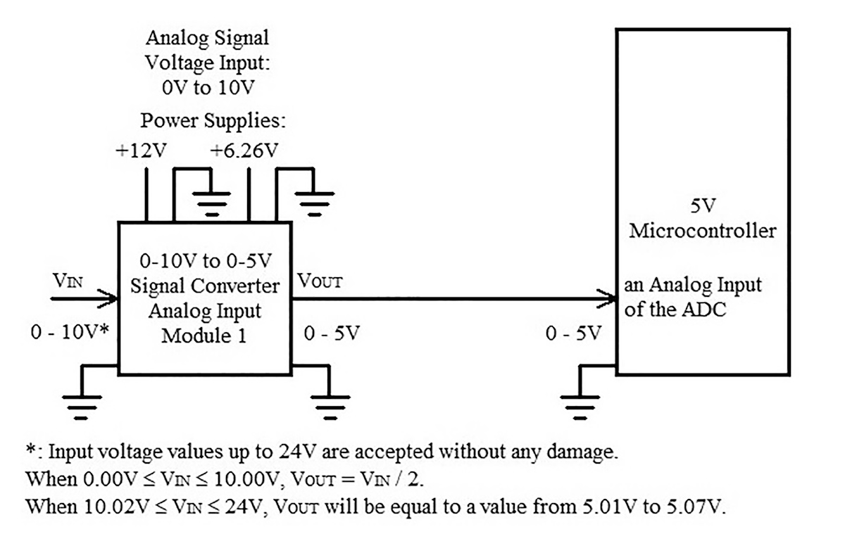
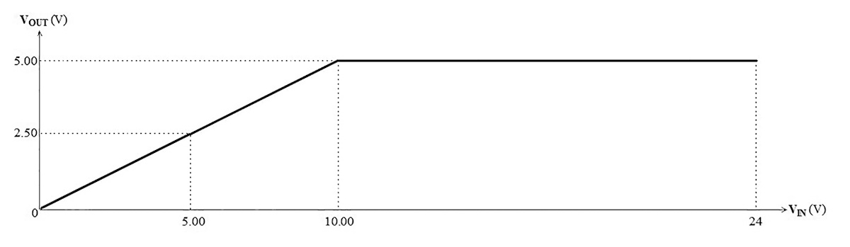
Figure 1 shows the schematic of the 0-10V to 0-5V Signal Converter, Analogue Input Module 1,with its connections shown in Figure 2. In this design it was assumed that the input voltage range (VIN) = 0.00V to 24V. When 0.00V ≤ VIN ≤ 10.00V, VOUT = VIN / 2. When 10.02 V – VIN – 24V, VOUT will be equal to a value from 5.01V to 5.07V, due to the electrical characteristics of the LM358P-A used. The relationship between VOUT and VIN is shown in Figure 3. It can be seen that input voltage values up to 24V are accepted without any damage to the circuit, and the output is a value from 5.01V to 5.07V.
Analogue voltage input signal VIN can be subjected to electric surge or electrostatic discharge on the external terminal connections. The TVS (transient voltage suppressor) shown in the circuit provides highly effective protection against such discharges. D1 is used to protect the circuit from accidental reverse polarity of VIN. A ferrite bead is connected in series with the input path to add isolation and decoupling from high-frequency transient noises. Resistors R1 and R2 divide down the input signal VIN into the range of 0V to 5V. External Schottky diodes generally protect the operational amplifier. Even when internal ESD protection diodes are provided, the use of external diodes lower noise and offset errors. Dual series Schottky barrier diodes D2 and D3 divert any overcurrent to the power supply or ground. The operational amplifier LM358P-A, with a +6.26V supply voltage, acts as a voltage limiter and is connected as a buffer amplifier (a voltage follower). VOUT is obtained from the output of the LM358P-A.
VIN(V) | VOUT(V) |
| 24.00 | 5.0X |
| .. | 5.0X |
| 20.00 | 5.0X |
| .. | 5.0X |
| 10.00 | 5.00 |
| .. | .. |
| 9.00 | 4.50 |
| .. | .. |
| 8.00 | 4.00 |
| .. | .. |
| 7.00 | 3.50 |
| .. | .. |
| 6.00 | 3.00 |
| .. | .. |
| 5.00 | 2.50 |
| .. | .. |
| 4.00 | 2.00 |
| .. | .. |
| 3.00 | 1.50 |
| .. | .. |
| 2.00 | 1.00 |
| .. | .. |
| 1.00 | 0.50 |
| .. | .. |
| 0.00 | 0.00 |
Table 1: Example input and output voltage values for the 0-10V to 0-5V signal converter, analogue ınput modules 1 and 2
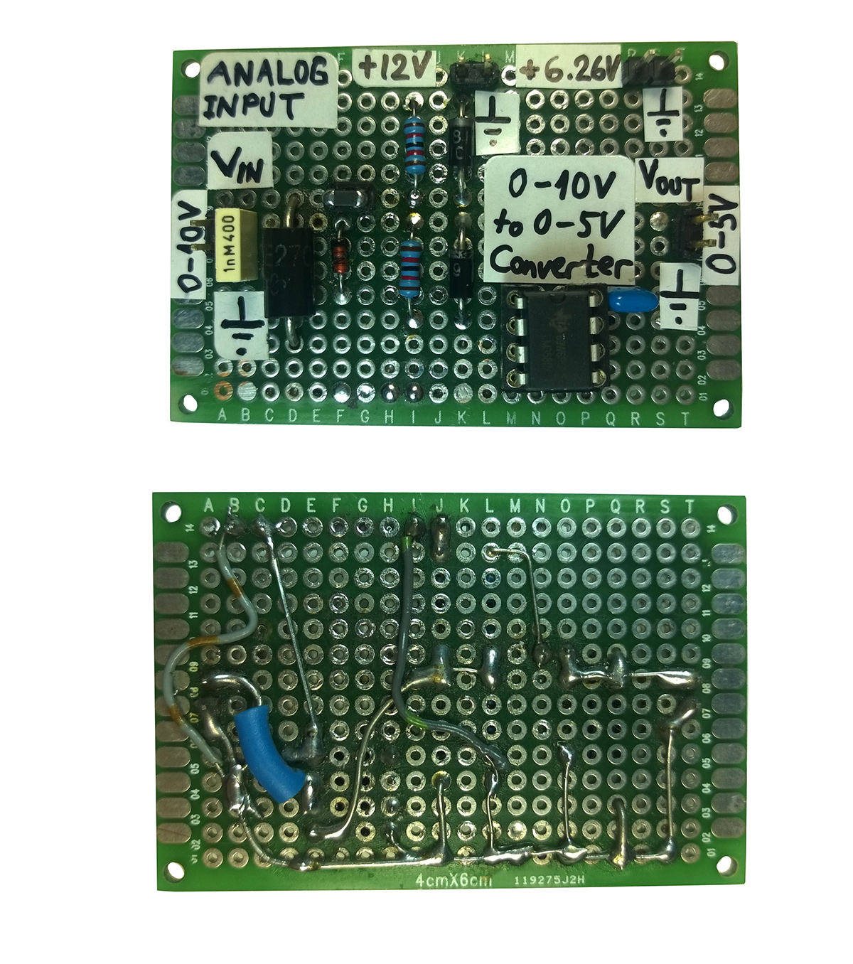
Table 1 shows example input and output voltages for this module, with top and bottom views of the prototype circuit board in Figure 4.
It’s worth noting that for proper operation, make R1 = R2.
0-10V to 0-5V Signal Converter – Analogue Input Module 2
Figure 5 shows the schematic of the 0-10V to 0-5V signal converter – analogue ınput module 2 for use with an ADC input of a 5V microcontroller; Figure 6 shows its connections. In this design as in the previous module it is assumed that the input voltage range (VIN) = 0.00V to 24V. When 0.00V ≤ VIN ≤ 10.00V, VOUT = VIN / 2. When 10.02 V ≤ VIN ≤ 24V, VOUT will be equal to a value from 5.01V to 5.07V, due to the electrical characteristics of the LM358P-1A used. The relationship between VOUT and VIN is shown in Figure 3.
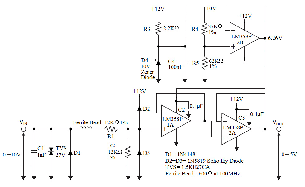
Except for the buffer amplifier LM358P-2A from where the output voltage VOUT is obtained, the lower part the schematic diagram is identical with that of the module 1. The upper part is dedicated to obtain the 6.26V reference voltage. R3, D4 (10V zener diode) and C4 provide a 10.00V reference voltage from a 12V power supply. Then, this 10.00V reference voltage is divided by using resistors R4 and R5 to obtain a 6.26V reference voltage. Next, the 6.26V reference voltage is connected to the non-inverting input of the buffer amplifier LM358P-2B, whose output is fixed as a 6.26V reference voltage, capable of sourcing up to 20mA.

Table 1 shows example input and output voltage values for this module, with views of its prototype circuit in Figure 7.

For proper operation, make R1 = R2 and R5/(R4+R5) = 62.62%.